Infineon launches industry-first SiC bidirectional switch built on 750 V CoolSiC G2 Technology
Infineon unveiled an industry-first 750 V CoolSiC G2 SiC bidirectional switch to simplify designs and boost efficiency/power density in EV charging and HVDC systems.
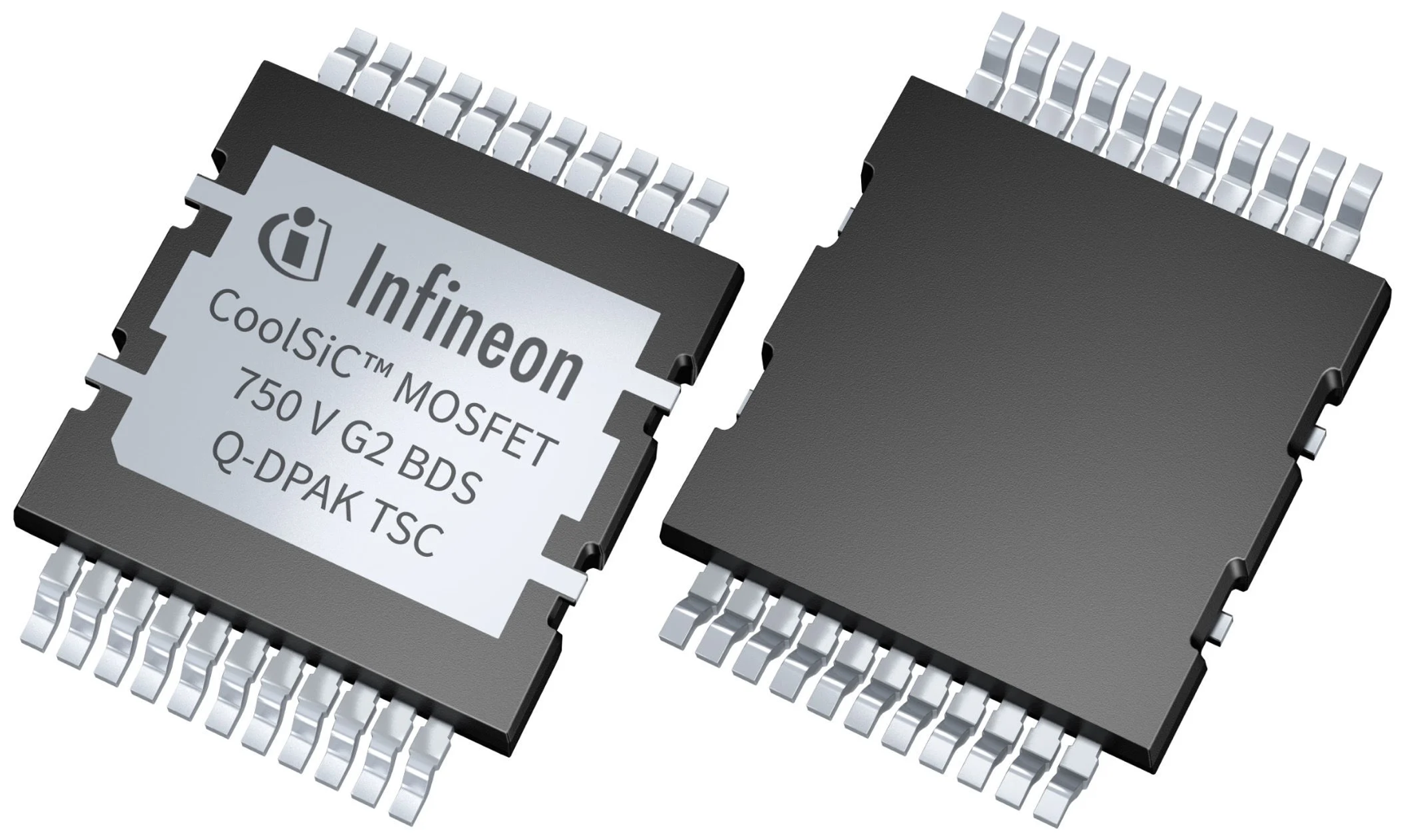
Infineon introduces a silicon carbide bidirectional switch portfolio built on its second‑generation 750 V CoolSiC platform, combining two dies in a common‑drain configuration and housed in a top‑side‑cooled Q‑DPAK. By integrating what would conventionally be two discrete power paths into one package, the devices aim to simplify bidirectional converter stages while pushing efficiency and power density in EV charging, on‑board chargers, and other high‑power systems.
SiC bidirectional switch built on 750 V CoolSiC G2 Technology
Vertically Integrated Common‑Drain Architecture for High‑Speed Switching
At the device level, the bidirectional switch is a vertically integrated dual‑die with a shared drain, enabling two power switches to operate as a single building block in bidirectional topologies. The G2 CoolSiC process targets low combined conduction and switching losses, underscored by figures of merit such as reduced RDS(on)×Qfr and improved RDS(on)×Qoss, along with a low total gate charge.
The gate system is tuned for noise immunity: a typical 4.5 V threshold at 25 °C and a very low QGD/QGS ratio help suppress unintended turn‑on under fast transients. For high‑frequency designs, the devices are rated to tolerate dv/dt slopes up to 200 V/ns, allowing rapid edges without compromising robustness. Extended gate‑bias transient tolerance from −11 V to +25 V broadens compatibility with a range of driver strategies and provides margin against ringing and system‑level perturbations.
Together, these characteristics support aggressive switching speeds in both hard‑ and soft‑switched stages while maintaining control over parasitic behavior.
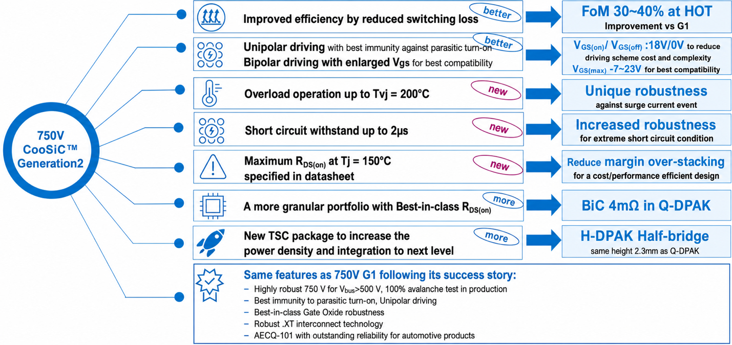
750V CoolSiC™ G2 builds on the outstanding performance of 750V G1
Device Ratings, Fault Tolerance, and Portfolio Granularity
Although positioned for 750 V applications, the family carries an 840 V drain‑source breakdown rating, offering margin when designers run bus rails at or above 500 V and must account for overshoot and surge.
Reliability under stress is emphasized: the devices are avalanche‑tested, specified for overload endurance at 200 °C for 100 hours, and include a short‑circuit withstand time of 2 µs—parameters that address fault cases such as inrush, load steps, or transient events on grid‑tied and storage systems. Initial on‑resistance options span from 14 mΩ up to 66 mΩ, enabling tradeoffs among conduction loss, thermal headroom, and silicon area as power‑stage requirements vary across applications.
These ratings collectively target durability in real operating environments rather than only bench conditions.
Top‑Side‑Cooled Q‑DPAK for Liquid‑Cooled Power Stages
Packaging is central to the platform’s objectives. By using a top‑side‑cooled Q‑DPAK, heat is routed directly from the die to a cold plate, which simplifies liquid‑cooling schemes and frees the PCB from shouldering the primary thermal path. This construction improves thermal resistance versus traditional bottom‑cooled surface‑mount layouts, enabling higher current per footprint or lower junction temperatures at a given load.
Infineon frames this bidirectional switch as an expansion of its top‑side‑cooled discrete family, targeting denser layouts and easier scaling where cold plates are already part of the mechanical design. For teams migrating from air‑cooled heat sinks to liquid‑cooled plates in compact racks or vehicle platforms, the package choice reduces the thermal design penalty typically associated with surface‑mount discretes.
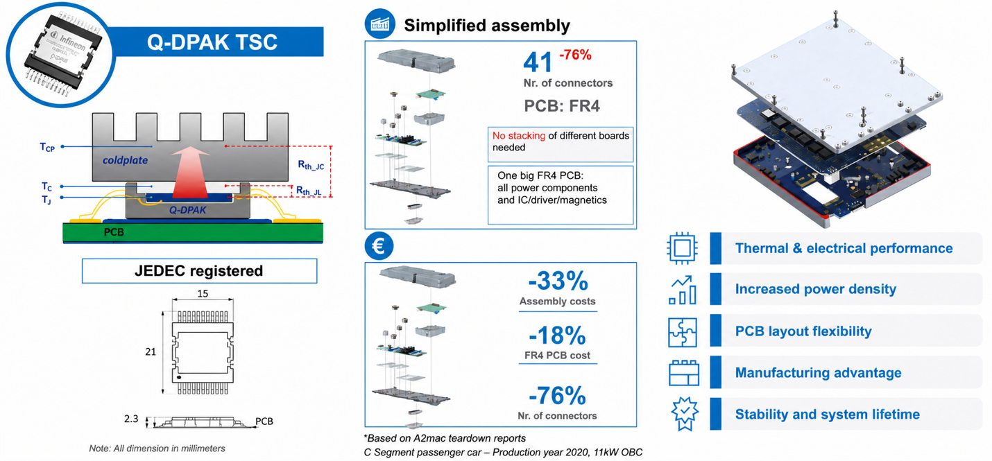
Top-side cooling facilitates enhanced thermal performance and contributes to notable reductions in manufacturing and BOM costs.
Implications for Converter Design and Gate‑Drive Choices
Because the device effectively consolidates two power transistors into a single common‑drain structure, it reduces interconnect parasitics relative to a board‑level pairing and can simplify current‑commutation paths in bidirectional legs.
The low QGD/QGS ratio and higher gate threshold reduce Miller‑induced turn‑on, which is often a limiting factor when pushing dv/dt and frequency in SiC stages. The wide transient gate‑bias window (−11 V to +25 V) also eases integration with existing SiC gate drivers that may see ringing or brief excursions during hard events, and it opens flexibility to optimize turn‑off voltage for immunity versus switching loss.
These behaviors matter in totem‑pole PFC, cycloconverter, and resonant stages where both halves of the cycle are actively controlled and edge rates drive EMI and efficiency trade‑offs.
Automotive Charging, eFuses, and Emerging HVDC Racks
In vehicles, the bidirectional SiC switch targets on‑board chargers and external charging equipment, with additional uses in solid‑state pre‑charge and eFuse functions where low loss, fast interruption, and thermal resilience are crucial.
Infineon notes that pairing the new device with its CoolSiC H‑DPAK half‑bridge can smooth the transition toward single‑stage OBC architectures based on SiC, a path that aims to cut component count and shrink magnetics while raising switching frequency.
On the industrial side, the company highlights liquid‑cooled high‑voltage DC supplies for AI servers, residential solar‑plus‑storage inverters, HVAC systems in hospitals or on‑premises data centers, eVTOL motor drive stages, and HVDC protection in power and IT racks. The breadth of applications reflects how a compact, thermally efficient, two‑way switch can replace discrete arrangements and reduce board complexity where bidirectionality and fast fault handling are mandatory.
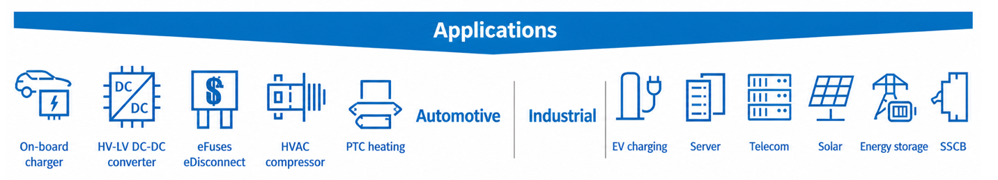
CoolSiC™ MOSFET 750 V G2 Automotive and Industrial Applications
Engineering Considerations and Next Steps
For power‑stage designers, the combination of a common‑drain SiC structure, high dv/dt capability, and top‑side‑cooled thermal path addresses three persistent bottlenecks at once:
- parasitics in bidirectional legs,
- gate‑drive‑limited switching speed, and
- heat extraction in compact assemblies.
The 840 V breakdown rating and short‑circuit endurance add the margin needed in electrified transport and rack‑scale HVDC systems where transient events are routine. With initial RDS(on) variants from 14 mΩ to 66 mΩ, the platform provides enough granularity to tune conduction losses against thermal design early in evaluation. Infineon plans to showcase the devices during PCIM Europe 2026 (June 9–11, Nuremberg), indicating near‑term ecosystem engagement around drivers and reference designs.
In short, Infineon’s 750 V CoolSiC G2 bidirectional switch brings a consolidated SiC building block—electrically fast, gate‑robust, and thermally optimized—that aims to simplify the next round of high‑power bidirectional converters across vehicles, renewables, and liquid‑cooled computing power.