Microchip Introduces 600 V Gate‑Driver Family for Motor Drives and Power Conversion
Microchip Technology introduced a 600 V gate-driver family featuring half-bridge, high/low-side, and three-phase options designed to simplify high-voltage motor drives and power conversion systems.
Microchip adds a 600 V gate‑driver family spanning half‑bridge, high‑/low‑side, and three‑phase options to address high‑voltage motor control and power conversion designs. Announced on January 21, 2026, the portfolio comprises a dozen devices with output‑drive choices from roughly 0.6 A to 4.5 A and logic compatibility down to 3.3 V, aiming to simplify interfaces to modern MCUs while improving robustness in noisy power stages. Target uses include motor drives and DC‑DC/AC‑DC conversion in industrial and consumer equipment.
600 V Level‑Shift Drivers with Bootstrap High‑Side Operation
At the core of the family is a high‑voltage level‑shift architecture that allows the high‑side output to ride on switching nodes up to 600 V using a bootstrap supply. A representative device, the MCP14H2184, drives a half‑bridge of N‑channel MOSFETs or IGBTs and specifies a recommended 10 V to 20 V bias for the gate‑drive supplies. The device accepts TTL/CMOS control inputs, including 3.3 V logic, and implements Schmitt‑triggered inputs with internal pulldown for noise immunity. An internal deadtime, nominally 400 ns, is included to prevent shoot‑through during high‑ and low‑side switchover.
For survivability at the switch node, the datasheet lists a dVs/dt transient rating of 50 V/ns, and undervoltage lockout monitors both high‑ and low‑side supplies with typical thresholds near 8.9 V. These details highlight suitability for off‑line inverter legs where rapid voltage edges and common‑mode transients are routine.
Topology Coverage and Drive‑Current Options
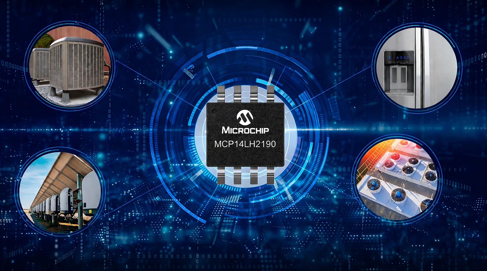
The 12‑part lineup is organized by drive topology and current capability so designers can align the driver to device gate charge and switching frequency targets. High‑/low‑side drivers such as the MCP14LH2101/2106 address discrete two‑switch legs, while higher‑drive variants (such as MCP14LH2190 and MCP14LH21904) scale to 4.5 A sink/source for fast charging and discharging of larger MOSFET and IGBT gates.
Half‑bridge devices include options with built‑in deadtime values; for example, Microchip lists versions with 100 ns or about 400 ns nominal delay to control overlap during commutation.
Packaging centers on SOIC‑8 and SOIC‑14 footprints for two‑switch stages, with a SOIC‑28 device supporting three‑phase motor applications. Across the family, logic‑level compatibility down to 3.3 V is emphasized to ease direct connection to common MCU and DSC GPIOs without additional level shifting.
For three‑phase systems, Microchip includes a device configured to drive six switches in a standard 3‑phase inverter bridge. While its per‑channel current is lower than the high‑drive discrete pair devices, it integrates the channel count and protections needed for compact BLDC/PMSM stage control. This arrangement can reduce board‑level complexity in appliances, pumps, fans, and other multi‑phase drives where the power devices have moderate gate charge and the switching frequency is set by acoustic and efficiency constraints.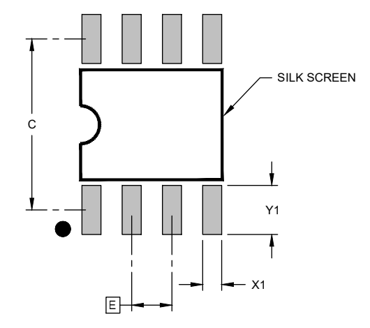
SOIC-8 Packaging
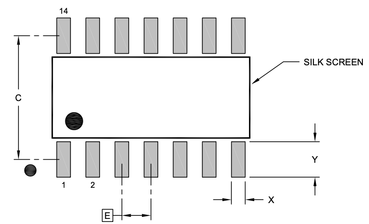
SOIC-14 Packaging
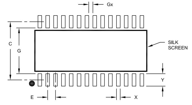
SOIC-28 Packaging
Noise Immunity, Protection Features, and Timing Behavior
The series places clear emphasis on operating margin in electrically harsh environments. Schmitt‑trigger inputs with defined thresholds help reject slow or noisy control edges from long signal traces or from controllers sharing a ground plane with high di/dt power loops.
Both high‑ and low‑side drivers include undervoltage lockout so the outputs remain off until the bootstrap and VCC rails are adequate—important for preventing partial enhancement and shoot‑through during start‑up or brownout events.
Negative transient tolerance at the outputs, along with the 50 V/ns offset‑slew rating in the half‑bridge device, addresses the practical reality of ringing and layout‑induced overshoot on the switch node.
From a timing perspective, the MCP14H2184 specifies typical turn‑on/turn‑off propagation delays of about 680 ns and 270 ns, respectively, with measured rise and fall times on the order of a few tens of nanoseconds into a 1 nF load. Internal deadtime is trimmed to roughly 400 ns with defined matching between the high‑ and low‑side paths, aiding predictable commutation without relying solely on firmware‑inserted blanking intervals.
These timing values are especially relevant when balancing switching losses against diode recovery and device capacitances in 100–200 kHz inverter legs or when synchronizing multiple phases in a vector‑controlled drive.
Engineers targeting faster switching or lower deadtime can select portfolio variants with different deadtime implementations or higher peak output current to move charge more quickly, subject to EMI and device stress limits.
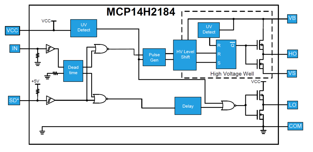
MCP14H2184 – Half-Bridge Gate Driver Block Diagram
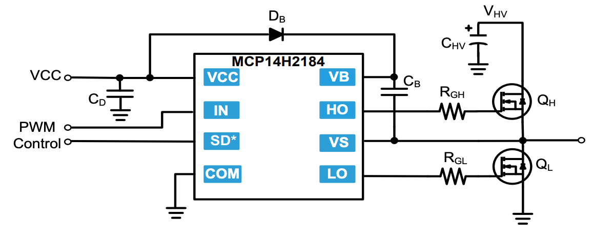
MCP14H2184 in a Half-Bridge Configuration
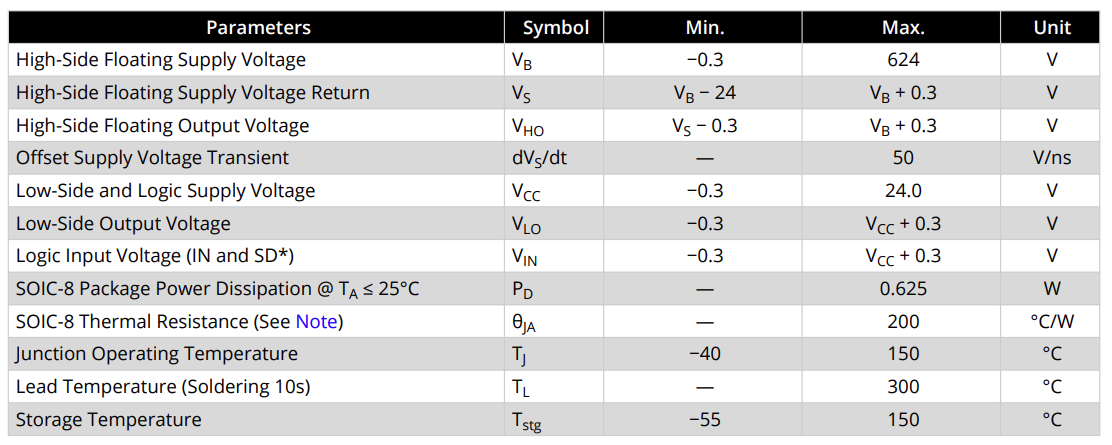
MCP14H2184 Electrical Characteristics – Absolute Maximum Ratings
System Integration and Design Implications
Direct 3.3 V logic support reduces interface components and level‑shifter delays, which is beneficial for digital current‑mode and FOC control loops that depend on deterministic timing between PWM edges and ADC sampling.
The availability of both modest (~600 mA) and higher (multi‑amp) drive strengths allows the same control architecture to scale from small motors and compact DC‑DC converters to larger inverter legs with higher gate charge devices.
For applications where the MOSFET or IGBT requires higher Miller‑plateau currents, the 4.5 A devices provide headroom to shorten transitions and reduce overlap losses, albeit with the usual care to manage EMI and dV/dt‑induced stress on isolation and sensors.
Package choices (SOIC‑8/14 for two‑switch stages and SOIC‑28 for three‑phase) simplify PCB routing, particularly around bootstrap networks and Kelvin‑connected source/emitters. Internal deadtime options reduce firmware dependency for shoot‑through prevention and can act as a safety backstop should control software misconfigure blanking times.
For offline supplies and inverter front‑ends built around ~400 V DC buses, the 600 V level‑shift margin aligns with typical worst‑case line and transient conditions, while still requiring careful snubbing and layout to contain overshoot and ringing. Microchip also makes simulation models available, enabling pre‑layout evaluation of gate‑drive current, timing, and bootstrap behavior before committing to prototypes.
Availability and Target Use Cases
According to Microchip, the family is in production and orderable, with parts positioned for a range of motor applications and power converters. The breadth of options—topology, deadtime, and drive strength—allows engineers to tailor a driver to the device technology (MOSFET vs. IGBT), switching speed, and efficiency objectives without redesigning the logic interface. Typical deployments include BLDC and PMSM drives, appliance compressors and pumps, compact industrial inverters, DC‑DC stages in auxiliary power supplies, and audio Class‑D amplifiers where a half‑bridge stage is common.
Microchip’s 600 V gate‑driver portfolio adds incremental but practical choices—level‑shift capability, defined deadtime options, and 3.3 V logic—that matter when closing the loop between a digital controller and a high‑voltage power stage.