Diamond Interposers Tackle Heat in GaN Power Amplifiers
MIT and collaborators embed GaN dielets in a single‑crystal diamond interposer to solve thermal bottlenecks, yielding a 4 W FR3 power amplifier with higher efficiency and reliability for next‑gen wireless and RF systems.
MIT and collaborators demonstrate a diamond-based thermal interposer that embeds GaN “dielets,” delivering multiwatt RF output with higher efficiency and headroom for next‑generation wireless front ends.
As wireless systems push toward higher power and wider bandwidths, engineers increasingly pair gallium nitride (GaN) transistors with silicon control and packaging layers to balance performance, integration, and cost. The drawback is heat: dense GaN devices generate localized hotspots that degrade reliability, limit output power, and diminish efficiency gains, especially in compact 3D heterogeneous assemblies.
An MIT-led team has addressed this choke point by embedding tiny GaN transistor “dielets” into an ultrathin single‑crystal diamond interposer that spreads heat laterally, equalizes device temperatures, and preserves transistor behavior. The group used the platform to build and measure a power amplifier that surpassed comparable designs reported in the literature, while relying on a fabrication flow positioned for scale-up as diamond wafer costs fall.
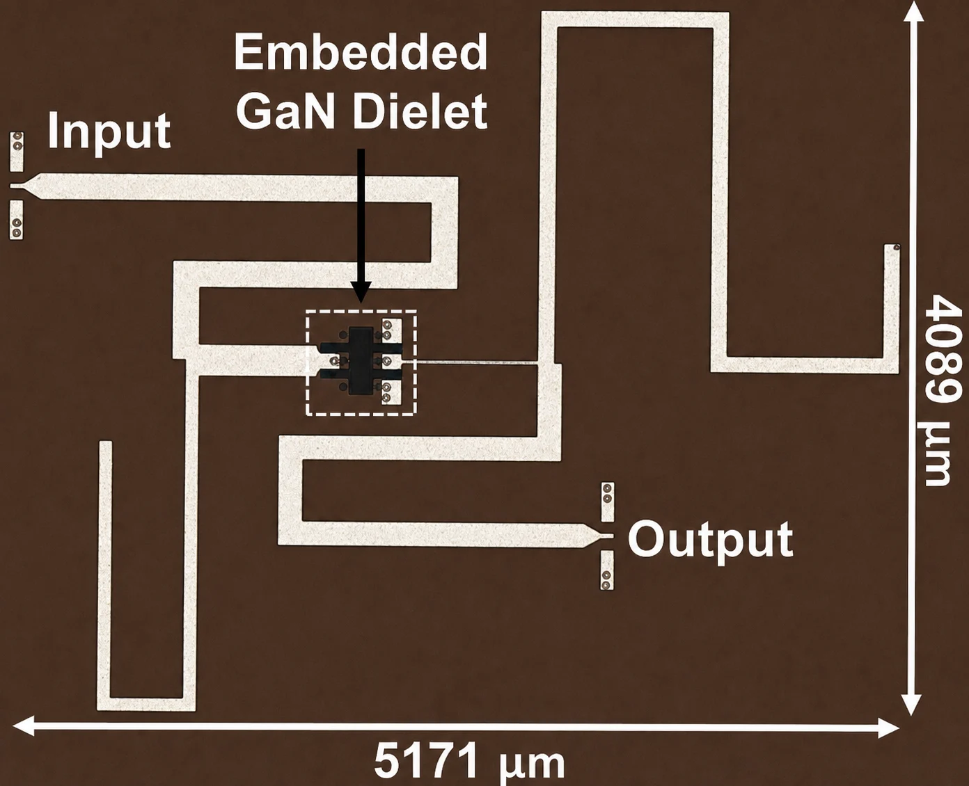
Fabricated heterogeneous power amplifier with embedded GaN-on-Si dielet in single crystal diamond interposer
Diamond as a Heat-Spreading Substrate Without Added Parasitics
Previous attempts to place diamond directly atop GaN have shown device‑level thermal relief but introduce additional capacitance and manufacturing complexity that can penalize RF performance and complicate high‑volume adoption. The MIT approach avoids those penalties by carving micron‑scale cavities into a thin diamond sheet and bonding singulated GaN dielets into the interposer.
After placement, the circuit is built up with dielectric and metallization layers to complete the RF signal path. Because the heat is extracted through the diamond, the GaN and silicon stack operate at more uniform temperatures, improving stability and enabling operation closer to each device’s intrinsic performance limits. The team reports that advances in lab‑grown, single‑crystal diamond have reduced material costs, improving the case for manufacturing.
From Femtosecond Dicing to a 4‑W FR3 Power Amplifier
The measured hardware centers on a heterogeneous power amplifier targeting the emerging 6G FR3 band around 8–10 GHz. Starting with GlobalFoundries 130RF GaN‑on‑silicon HEMTs, the researchers used femtosecond‑laser dicing to create roughly 274 μm × 400 μm single‑transistor dielets, then thinned and prepared them for integration.
Each dielet was bonded into a blind cavity in the diamond using a high‑thermal‑conductivity die‑attach film under 2 N force at 150 °C for 30 minutes, forming the primary thermal interface. A two‑layer redistribution stack—implemented with 15 μm Ajinomoto build‑up film (ABF GL102) and 4 μm copper—completed the interposer metallurgy for circuit construction. Keysight ADS and Ansys HFSS were employed for co‑design of the device, package, and matching networks.
In large‑signal characterization, the interposer platform improved the dielet’s load‑pull behavior and yielded higher output power, power‑added efficiency (PAE), and gain at 10 GHz compared with the same device before embedding. The finished amplifier delivered up to 4 W output with a 3 dB bandwidth from 6.8 to 10.3 GHz and sustained 39–49% PAE across 8–10 GHz, with backed‑off operation characterized for high peak‑to‑average ratio signals. Stability metrics (K and μ > 1) indicated unconditional stability in the operating band.
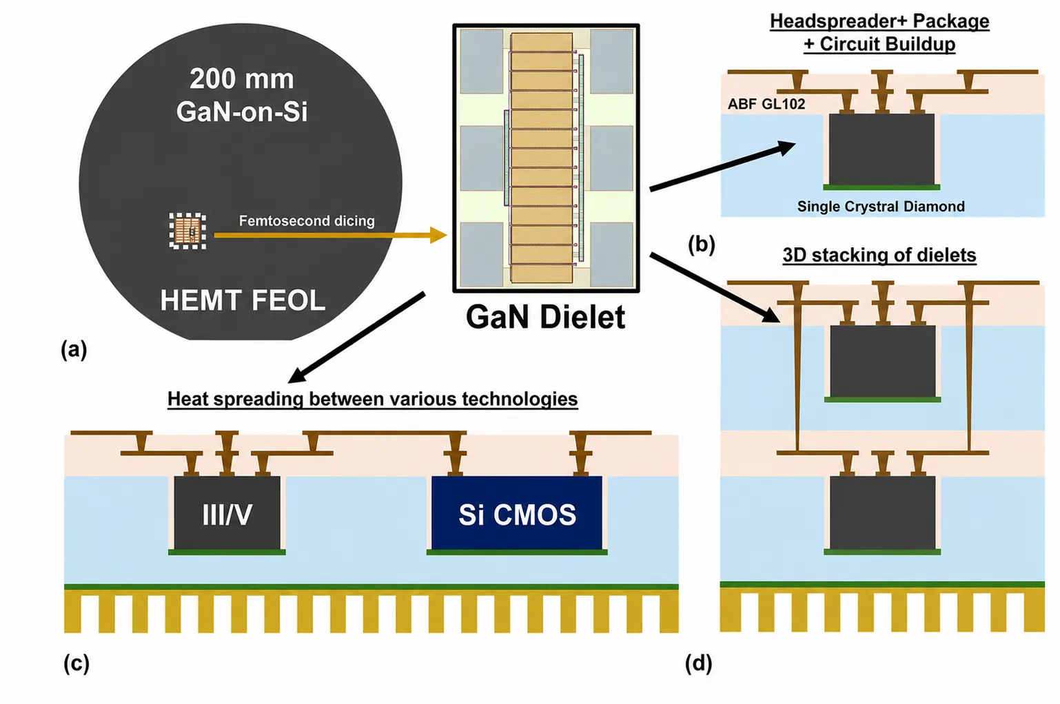
Heterogeneous GaN in single crystal diamond interposer roadmap. (a) Dielet fabrication using femtosecond laser. (b) Power amplifier buildup in diamond interposer. (c) Heterogeneous integration of III-V’s and Si CMOS in diamond interposer. (d) Heat spreading solution for 3D PAs
Bridging Reliability and Performance in 3D Heterogeneous Integration
The result matters beyond single‑device benchmarks. In tightly stacked RF front ends—where GaN, silicon, and other materials share limited thermal headroom—temperature gradients drive drift, stress, and lifetime concerns. A diamond interposer that doubles as both heat spreader and circuit substrate offers a practical means to lower junction temperatures without adding top‑side parasitics, helping maintain gain linearity and efficiency under load.
In the MIT study, the diamond layer normalized thermal conditions sufficiently to realize measurable RF gains versus the same transistors in more conventional builds, demonstrating that thermal design can directly translate into electrical performance improvements at the circuit level.
The team further emphasizes that the technique is compatible with the kind of precision pick‑and‑place and multilayer processing used in advanced packaging lines, pointing toward manufacturability.
Operational Impact for Wireless Infrastructure and High‑Power Systems
A scalable diamond‑interposer path has several implications for system architects. For base stations and phased‑array front ends working in mid‑to‑upper microwave bands, multiwatt PAs with improved PAE reduce thermal design margins and power delivery demands at the radio unit, directly affecting cooling plant sizing and enclosure constraints.
For aerospace and space links, higher power density at a given mass can extend link budgets or enable smaller apertures and lighter platforms. Industrial drones and high‑duty‑cycle radar nodes benefit from the added efficiency headroom and thermal robustness in congested, thermally challenged nacelles.
The researchers also point to applications in power conversion hardware inside data centers, where temperature management at high current density is an ongoing limiter; diamond interposers could provide a route to keep conversion stages compact while controlling hotspots that drive derating. While these are application‑level inferences, the measured amplifier performance and the thermal‑electrical co‑design approach provide an engineering basis for such system gains.
Integration Details That Matter to Manufacturing Engineers
Several aspects of the reported flow are notable for engineers considering technology transfer.
- First, by starting with commercial GaN‑on‑Si HEMTs and singulating to dielets, the approach leverages existing wafer supply and process control, avoiding a bespoke GaN‑on‑diamond growth step that can raise defectivity and parasitics.
- Second, the thermal interface process uses modest pressure and temperature, which helps maintain device integrity and keeps the sequence compatible with backend packaging constraints.
- Third, the interposer’s two RDL layers and microstrip matching networks illustrate that the diamond substrate can host practical RF layouts without exotic processing, easing adoption in multi‑chip modules.
- Finally, the reported improvement in load‑pull characteristics after embedding suggests that the interposer can stabilize device behavior under large‑signal drive—useful for meeting linearity and spectral mask requirements in modern modulations.
Together, these elements set a credible path from lab demonstrator to pilot‑line evaluation.
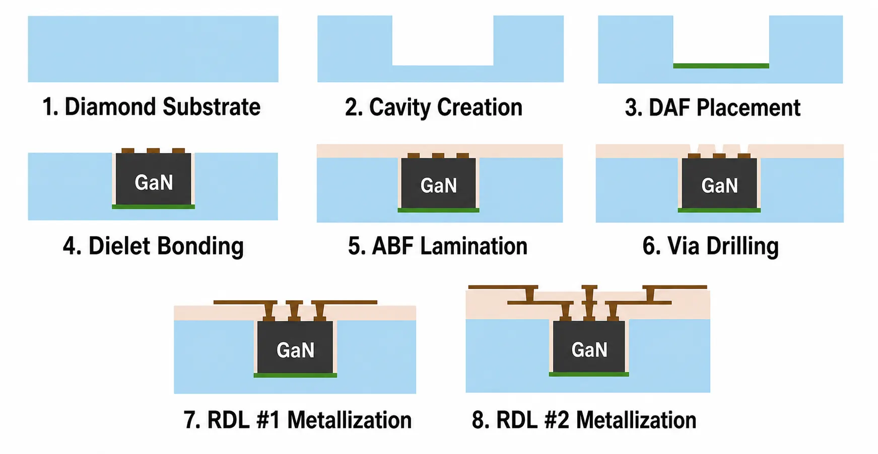
Fabrication process of diamond interposer
Industry Significance
GaN has long promised higher power and efficiency for wireless and radar systems, but packaging and thermal limits have constrained the practical envelope in compact, integrated front ends.
By demonstrating a diamond interposer that both removes heat and supports RF circuit build‑up, the MIT‑led team shows a route to extract more of GaN’s intrinsic performance without paying a parasitic penalty.
The measured 4‑W, FR3‑band amplifier and its efficiency profile make a concrete case that thermal architecture belongs alongside transistor physics and matching topology in the RF engineer’s performance budget.
If diamond wafer availability and interposer process integration continue to mature, this platform could influence how vendors design radio units for 6G‑class infrastructure, satcom terminals, high‑power radars, and other thermally limited electronics.