Understanding the Practical Challenges of GaN Power Devices
Learn about the device-level and application-level challenges that influence the performance, reliability, and practical adoption of GaN power devices.
GaN has several advantages over SiC technology including higher bandgap energy as well as higher electron mobility. GaN's application, however, has been limited as compared with SiC‐MOSFETs. One of the key reasons for that is GaN's lower thermal conductivity. Therefore, GaN has limited capability in higher power applications where more heat needs to be dissipated.
Figure 1 provides an insight into the region in terms of power and frequency where GaNs can be most effective. As shown in Figure 1, GaNs are best fitted into applications with up to 10 kW power and >100 kHz switching frequency. In transportation electrification, this specification mainly involves DC–DC converters and on‐board chargers (OBCs). These are the primary application targets for GaNs in transportation electrification.
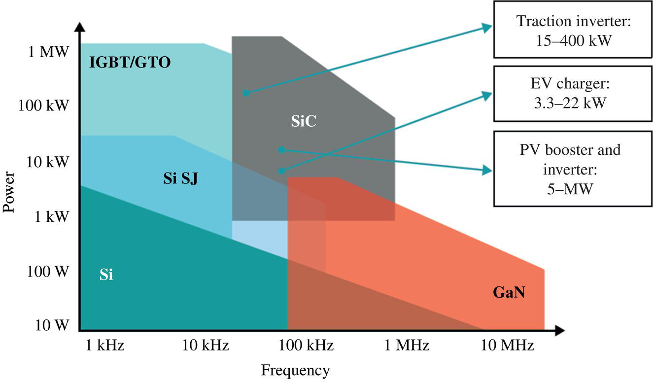
Figure 1 Semiconductor device application based on power and frequency range.
While GaN power devices can provide system‐level benefits in certain applications, there are challenges associated with GaNs that have limited their further penetration into the transportation electrification market. These challenges can be classified into two main categories:
- Device Physics Level
- Application Level
Device Physics Level Challenges with GaNs
Device physics level challenges associated with GaN power devices are the ones that originate from the device architecture and its specific characteristics. These issues include electron trapping, punch‐through current, and substrate lattice and CTE mismatch.
Electron Trapping
The known inverse piezoelectric effect in GaNs device architecture is the main root cause for electron trapping. The trapped charges normally accumulate close to gate, source, and drain edges when the device is exposed to an external electric field. The trapped charges adversely impact device performance by introducing excessive leakage currents.
One of the major issues caused by electron trapping is the dynamic increase in channel resistance, Ron, as a result of trapped charge leakage proceeding from the gate edge to the drain edge. This phenomenon is also known as current collapse.
Gate Edge Degradation
The structural defects such as inverse piezoelectric effect, time‐dependent trap formation, percolative conductive path formation, electrochemical reactions, and gate metal diffusion result in failure mechanisms in GaN/AlGaN layer. These defects occur next to the gate edge of the GaN power device where the electric field strength is maximum. That, in turn, results in electrons tunneling from the gate edge into the AlGaN barrier layer and, therefore, increasing the gate leakage current. This not only adversely affects the output power and efficiency but also reduces the device's reliability.
Punch Through Current
The source to drain leakage is also called punch‐through current and is primarily caused by defects in GaN and buffer layers. As shown in Figure 2, the charge from the source leaks to the drain by taking an alternate path through the GaN layer. Such behavior can only be observed when the device is in its semi‐OFF state.
Substrate Choice
Although the bulk GaN layer as a substrate improves the device performance, the fabrication process of bulk GaN multilayers is a complex task and commercially not a feasible choice. Therefore, as shown in Figure 2, an alternative technique is used for device fabrication where GaN is grown over substrates such as Si, sapphire, and SiC. The challenge associated with this approach is the lattice and coefficient of thermal expansion (CTE) mismatch between GaN and the substrate material.
Table 1 compares the lattice and CTE values for GaN vs various potential substrate materials. SiC offers better characteristics with a 3.5% lattice mismatch. But the 33% of CTE mismatch between GaN and SiC is still significant and can cause problems as the devices go through power cycling in the application. Not to forget that SiC is more expensive compared with Si.
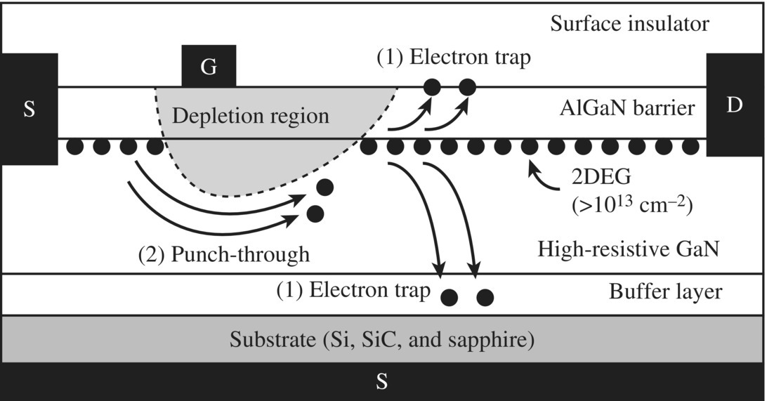
Figure 2 Device‐level issues of GaN: (1) electron trapping and (2) punch‐through current.
|
Substrate |
GaN |
Si <111> |
Sapphire (Crystal of Al₂O₃) |
SiC 6H |
Ge <111> |
|
Lattice Constant |
3.19 |
3.84 |
2.75 |
3.08 |
4.0 |
|
Coefficient of Thermal Expansion (CTE) |
5.6 |
2.6 |
7.5 |
4–4.2 |
5.9 |
Table 1 Lattice constant and CTE of semiconductor material.
Application Level Challenges with GaNs
Other than the device physics level challenges associated with GaNs, there are also application‐/circuit‐level challenges for GaN power devices. Below is a summary of challenges associated with GaNs in the application level.
GaN's Narrow Gate Voltage Margin
Figure 3 shows the output characteristics of EPC2001C GaN device. As seen here, the device is fully enhanced at a gate voltage of 5 V. Table 2 shows the EPC2001C absolute maximum ratings. Based on Table 2, the absolute maximum permissible gate voltage is only 6 V, which means there will be only a 1 V safety margin with respect to the nominal gate voltage of 5 V. Therefore, the gate driver design must include special considerations to limit the voltage overshoot across the gate‐to‐source terminals.
Other than the device parasitic elements, this overshoot also depends significantly on gate loop stray inductance. Therefore, an optimized circuit layout becomes significantly more important in GaN applications as compared with silicon applications where the safety margin is much wider.
There are various other ways to mitigate the VGS overshoot problem including adding an external capacitor in parallel with CGS and/or adding a gate resistor to the gate loop. Note, however, that both of these two techniques will increase the device‐switching loss and will limit the maximum operating switching frequency.
Placing a Zener diode‐based clamp circuit in parallel to the gate is an alternative technique that can be utilized to limit the gate voltage overshoot. The non‐linearity of the Zener diodes, however, adds complexity to the design and, therefore, this technique is less preferred. Despite all these techniques, GaN power devices still suffer from overshoots during turn‐on events that can result in catastrophic failures.
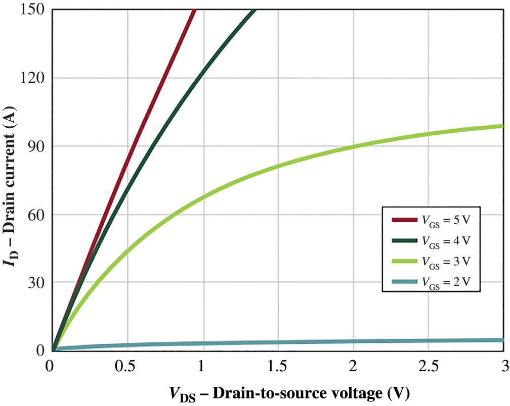
Figure 3 EPC2001C output characteristic curves.
|
Symbol |
Parameter |
Value |
Unit |
|
VDS |
Drain-to-source voltage (continuous) |
100 |
V |
|
VDS |
Drain-to-source voltage (up to 10,000 pulses of 5 ms at 125°C) |
120 |
V |
|
ID |
Continuous current (TA = 25°C, θjA = 13) |
36 |
A |
|
ID |
Pulsed current (25°C, TPulse = 300 μs) |
150 |
A |
|
VGS |
Gate-to-source voltage (positive) |
6 |
V |
|
VGS |
Gate-to-source voltage (negative) |
−4 |
V |
|
Tj |
Operating temperature range |
−40 to 150 |
°C |
|
Tstg |
Storage temperature range |
−40 to 150 |
°C |
Table 2 EPC2001C absolute maximum ratings.
The other characteristic associated with a narrow gate voltage margin in GaN power devices is the RDS(on) change by a small variation in gate voltage. Figure 4 shows the typical RDS(on) change by gate voltage in EPC2001C.
As seen in Figure 4, with gate voltages of <4 V, a small change in gate voltage results in a significant change in RDS(on). For example, looking at the ID = 80 A curve, reducing the gate voltage from 4 to 3.5 V, the RDS(on) increases by ~28%. Therefore, special care must be taken to the design of the gate driver board such that not only the VGS overshoot is tightly controlled but a tight voltage regulation is also achieved.
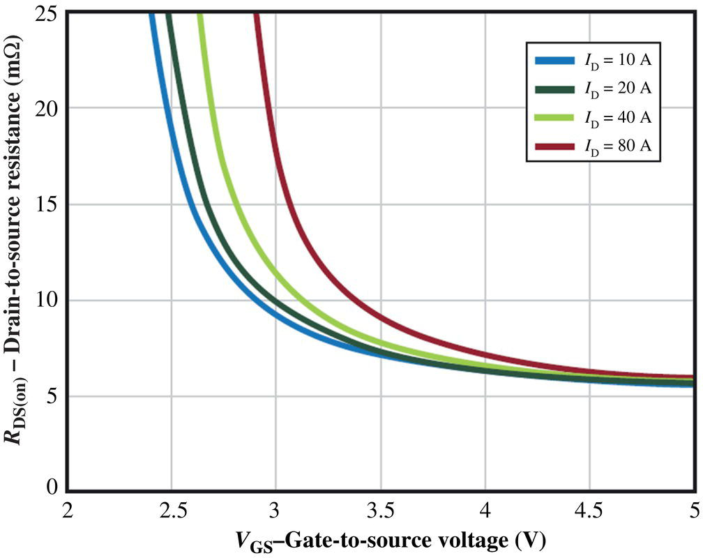
Figure 4 Effect of dv/dt – RDS(on) vs VGS for various drain currents for EPC2001C.
dv/dt Immunity and False Turn‐On in GaN Devices
A typical GaN power device including its parasitic capacitance is shown in Figure 5. In this figure, as the device turns off, it faces a high dv/dt slew rate across its drain to the source. This high dv/dt, in turn, rapidly charges the device's parasitic capacitances as illustrated in Figure 5. The charge current passing through the gate will raise the gate voltage. If the gate voltage is raised beyond its threshold limit, it can falsely turn the device on. This phenomenon is also called the Miller effect and can cause shoot‐through in half‐bridge architectures.
Note that the same phenomenon exists in silicon devices as well as SiC‐MOSFETs. However, the issue is worse in the case of GaN power devices as the turn‐on threshold voltage is lower in the case of GaN devices. For example, the minimum threshold voltage in the case of EPC2001C is only 800 mV.
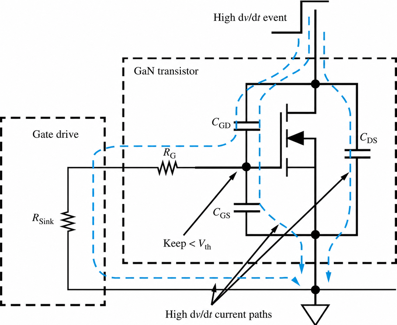
Figure 5 Effect of dv/dt on a GaN device in the off‐state.
di/dt Immunity in GaNs
Figure 6 shows how the step voltage induced across the common source inductance (CSI) as a result of high di/dt can induce an opposing voltage across the gate‐to‐source of a GaN device in the off state. The induced voltage across the gate‐to‐source is a negative voltage, which, if not damped properly, can cause ringing due to the RLC tank created in the gate loop.
If the positive voltage created as a result of ringing at the gate goes beyond the device threshold, it can falsely turn it on and cause a shoot‐through.
Note that this phenomenon is also present in all other switching devices. However, the outcome is more severe in the case of GaNs as GaN's turn‐on threshold voltage is lower as compared with other switching devices such as silicon and silicon carbide.
In addition to that, as seen in Table 2, the absolute maximum permissible voltage is limited to a positive voltage of 6 V and a negative voltage of –4 V. Therefore, not only the positive ringing across the gate‐to‐source can cause false turn‐on and shoot‐through but the negative ringing across the gate‐to‐source can also exceed device limitations and cause catastrophic failure.
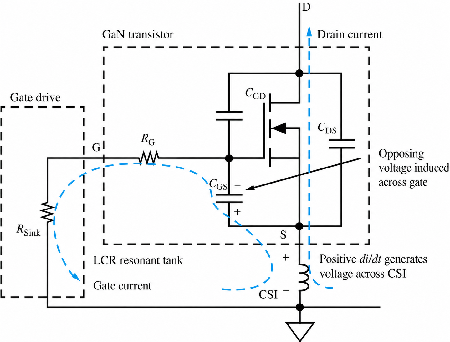
Figure 6 Impact of a positive di/dt of an off‐state device with common‐source inductance.
One potential solution to this issue is to increase the damping in the gate loop in off‐state by increasing the sink resistor, RSink, in Figure 6. However, increasing the gate loop sink resistor would negatively impact the dv/dt immunity, which can also cause false turn‐on. Therefore, the di/dt immunity still remains a challenge with GaNs in practical applications.
While these are some of the key challenges associated with GaNs in both the device level and application level, efforts are being made to address these issues so the benefits associated with GaNs can be utilized in transportation electrification.
Key Takeaways
GaN power devices are particularly well suited for high-frequency applications such as DC-DC converters and onboard chargers, but their lower thermal conductivity and narrow gate voltage margin create unique design challenges. Device-level issues including electron trapping, current collapse, gate degradation, punch-through current, and substrate mismatch can affect efficiency and long-term reliability. At the application level, designers must carefully manage gate voltage overshoot, RDS(on) sensitivity, dv/dt-induced false turn-on, and di/dt ringing caused by parasitic inductances. Although these challenges are actively being addressed, successful GaN implementation requires optimized device structures, gate-driver design, and PCB layout techniques.