Exploring n-Type and p-Type Metal Oxide Semiconductors
Learn about the properties, crystal structures, and applications of major n-type and p-type metal oxide semiconductors used in electronics, optoelectronics, sensors, and energy devices.
Metal oxide semiconductors (MOS) are abundant materials found in the Earth's crust and are commonly used in traditional ceramics. However, they differ significantly from conventional inorganic counterparts like silicon and III–V compounds in various aspects.
These distinctions encompass materials design concepts, electronic structure, charge transport mechanisms, defect states, thin-film processing, and optoelectronic properties. As a result, oxide semiconductors enable the realization of both established and innovative functionalities.
In comparison to inorganic semiconductors, oxide semiconductors possess unique characteristics. These include:
- exceptional carrier mobilities even in the amorphous state,
- resilience against mechanical stress,
- compatibility with organic dielectric, and
- photoactive materials, and high optical transparency
These properties make oxide semiconductors particularly appealing for various applications.
In recent decades, MOS have garnered significant attention in various research fields, including optoelectronics, thin-film transistors (TFTs), photocatalysts, gas sensors, solar cells, and memristors, as shown in Figure 1.
MOS can be categorized into two types based on their conductivity: n-type, where electrons are the majority carriers, and p-type, where holes are the majority carriers. These semiconducting properties arise from factors such as doped aliovalent cations or oxygen nonstoichiometry.
Among the n-type MOS, ZnO, SnO2, TiO2, In2O3, and Ga2O3 are widely studied concerning synthesis, characterization, and applications. As for the p-type MOS, research efforts primarily focus on CuxO (CuO and Cu2O), SnO, and NiOx.
n-Type Metal Oxide Semiconductors
ZnO
Zinc oxide (ZnO), as an n-type semiconductor, has sparked significant research interest due to its distinctive physical and chemical properties. In the field of materials science, ZnO is classified as an II–VI compound semiconductor, possessing a covalence level between ionic and covalent semiconductors. Its attributes, such as a direct wide bandgap (Eg ∼ 3.3 eV at 300 K), large free exciton binding energy (60 meV), and high thermal and mechanical stability at room temperature, make ZnO a promising candidate for various applications in electronic devices, optoelectronics, gas sensors, and laser technology.
Additionally, ZnO can be utilized as an energy collector due to its piezo- and pyroelectric properties, as well as a photocatalyst for hydrogen production.
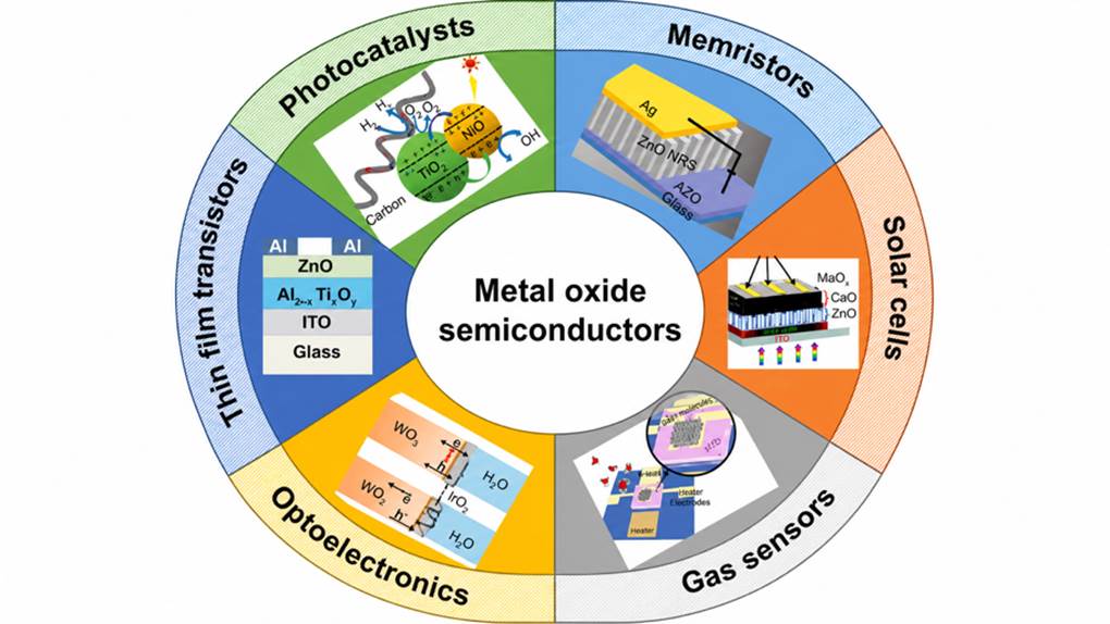
Figure 1 Applications of metal oxide semiconductors.
The crystal structure of ZnO can be classified into three types:
- wurtzite (B4),
- zinc blende (B3), and
- rocksalt (B1), as shown in Figure 2.
Wurtzite is the most stable thermodynamic phase under ambient conditions. Wurtzite ZnO possesses a hexagonal structure (space group C6mc) with lattice parameters a = 0.3296 nm and c = 0.52065 nm.
The structure of ZnO can be simply described as a number of alternating planes composed of tetrahedrally coordinated O2− and Zn2+ ions, stacked alternately along the c-axis. The tetrahedral coordination in ZnO results in noncentral symmetric structures and consequently piezoelectricity and pyroelectricity.
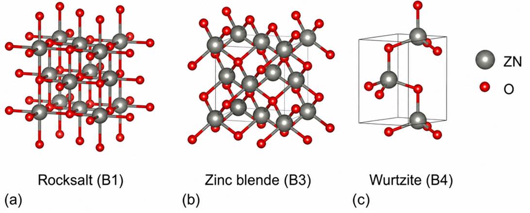
Figure 2 Stick and ball representation of ZnO crystal structures: (a) cubic rocksalt (B1), (b) cubic zinc blende (B3), and (c) hexagonal wurzite (B4). The gray and red spheres denote Zn and O atoms, respectively.
SnO2
SnO2 is also a wide-bandgap (∼3.6 eV) n-type semiconductor, belongs to the group-IV compounds, and exhibits remarkable transparency and conductivity simultaneously. The unique chemical, electronic, and optical properties of SnO2 have led to extensive research on its applications in various devices, including solar cells, catalytic materials, and gas sensors.
Additionally, SnO2 serves as a distinctive transparent metal oxide and finds wide-ranging applications as transparent conducting oxide electrodes in optoelectronic devices. This is due to its excellent chemical and thermal stabilities in atmospheric environments, as well as its high optical transmission properties.
SnO2 possesses several polymorphs including:
- rutile-type ($P_{4_{2}}/mnm$),
- CaCl2-type (Pnnm),
- a-PbO2-type (Pbcn),
- pyrite-type ($Pa\bar{3}$),
- ZrO2-type orthorhombic phase I (Pbca),
- fluorite-type ($Fm\bar{3}m$), and
- cotunnite-type orthorhombic phase II (Pnam) with ninefold coordination, as shown in Figure 3.
All these structures are sequentially obtained when the most commonly available and stable rutile phase is subjected to a high mechanical pressure.
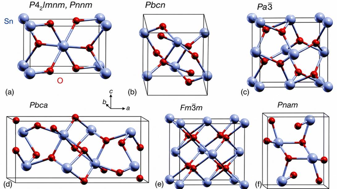
Figure 3 Bulk structures of SnO2 polymorphs (gray and red colors represent Sn and O atoms, respectively). (a) Rutile ($P_{4_{2}}/mnm$) and CaCl2-type (Pnnm), (b) R-PbO2-type (Pbcn), (c) pyrite-type (Pa), (d) ZrO2-type (Pbca), (e) fluorite-type (Fmhm), and (f) cotunnite-type (Pnam).
In2O3
Another widely studied n-type semiconductor is indium oxide (In2O3), which has a bandgap ranging from 3.5 to 3.7 eV. It finds numerous applications in electronic and optoelectronic fields such as solar cells, gas sensors based on TFTs, and Schottky contacts and diodes. In2O3 can exist in two well-established crystal structures:
- body-centered cubic (bcc) and
- rhombohedral (rh), as depicted in Figure 4.
The phase of In2O3 thermodynamically stable under ambient conditions adopts the body-centered cubic bixbyite structure, with the space group $Ia\bar{3}$ (#206) and a lattice constant of 10.118 Å. The rhombohedral structure is stabilized under high-pressure conditions. The rhombohedral cell belongs to the $R\bar{3}c$ space group with lattice constants a = 5.478 Å and c = 14.51 Å.
There are six formula units per hexagonal cell, and the volume per formula of 62.85 Å3 for the rh phase is much smaller than the value of 64.72 Å3 for the ambient bcc phase.
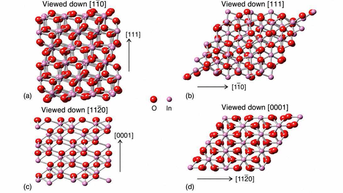
Figure 4 Ball and stick representations of crystal structures of bcc-In2O3 (a, b) and rh-In2O3 (c, d). In atoms are pale pink, and O atoms are dark red. The viewing directions and the in-plane orientation are indicated in the figure.
TiO2
As a member of transition metal oxides, TiO2 is a well-known n-type semiconductor. It exhibits excellent electronic and optical properties, making it highly suitable for various applications in the fields of gas sensors, solar cells, and photocatalysis. In its natural form, TiO2 exists in three different phase structures, namely
- anatase (tetragonal),
- brookite (orthorhombic), and
- rutile (tetragonal), as illustrated in Figure 5.
These phases have energy bandgaps of 3.2 eV (anatase), 3.02 eV (brookite), and 2.96 eV (rutile). Among these phases, anatase and rutile are widely applied due to their superior stability, while rutile TiO2, with a tetragonal structure containing six atoms per unit cell, exhibits a slight distortion in the TiO6 octahedron.
Anatase TiO2 also possesses a tetragonal structure, but with a slightly larger distortion of the TiO6 octahedron. In general, rutile TiO2 is more thermodynamically stable than anatase under typical temperature and pressure conditions.
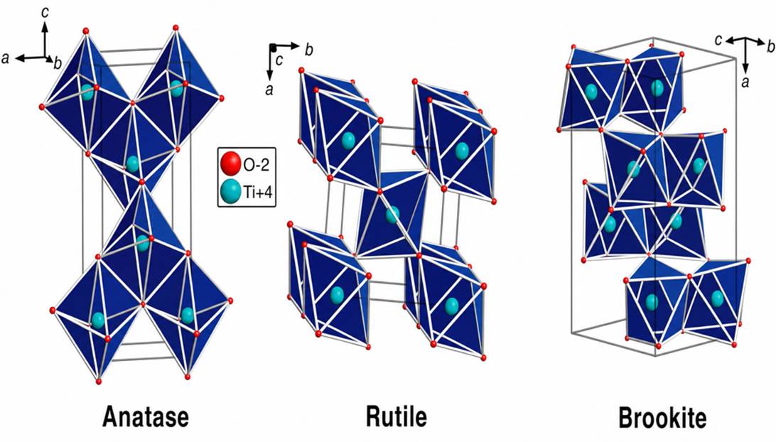
Figure 5 Structure of anatase, rutile, and brookie TiO2.
Ga2O3
Ga2O3 is an emerging ultra-wide bandgap semiconductor with a bandgap of 4.8 eV. This unique property enables Ga2O3 to simultaneously achieve high breakdown voltage and low on-resistance, making it highly promising for both direct current (DC) and radiofrequency (RF) applications. As a result, Ga2O3 offers exciting prospects in various fields such as electronics (high-power devices, field-effect transistors), optoelectronics (solar cells, solar-blind ultraviolet photodetectors), and sensors (gas sensors, radiation detectors).
Ga2O3 exists in five polymorphs, including:
- corundum (α),
- monoclinic (β),
- defective spinel (γ),
- orthorhombic (δ), and
- hexagonal (ε), as shown in Figure 6.
Among these, β-Ga2O3 is the most stable phase under ambient conditions, while the other phases can transform into β-Ga2O3 through heating treatment.
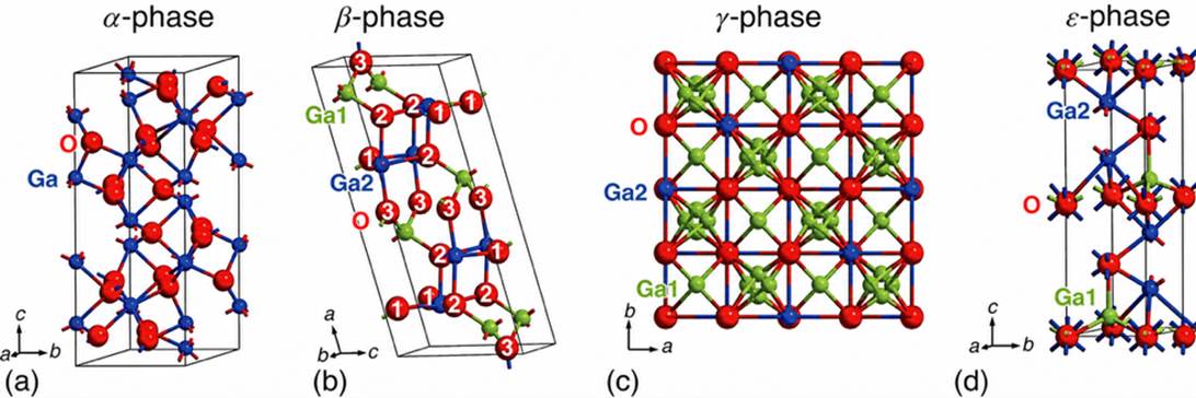
Figure 6 Crystal structure Ga2O3 polymorphs. (a) Rhombohedral crystal structure of corundum-like α-Ga2O3. (b) Monoclinic β-Ga2O3 crystal structure. (c) Cubic defective spinel lattice structure of γ-phase Ga2O3. (d) Orthorhombic ε-Ga2O3 structure.
p-Type Metal Oxide Semiconductors
Copper Oxides (CuO/Cu2O)
Tenorite (CuO) and cuprite (Cu2O) are two stable phases in copper oxides at an ambient environment. As p-type semiconductors, CuO and Cu2O separately possess a band gap of 1.9–2.1 and 2.1–2.6 eV. Both binary copper oxides are attractive for versatile applications such as solar cells, TFTs, gas sensors, and photoelectric detectors. When annealed at a high temperature, Cu2O could transform to CuO by the oxidation reaction.
In addition to these two stable phases, paramelaconite (Cu4O3) is another metastable mixed-valence intermediate compound between Cu2O and CuO and could decompose into Cu2O and CuO beyond the stability limit under vacuum environment at 670–800 K. Figure 7 illustrates these crystal structures of Cu2O and CuO.
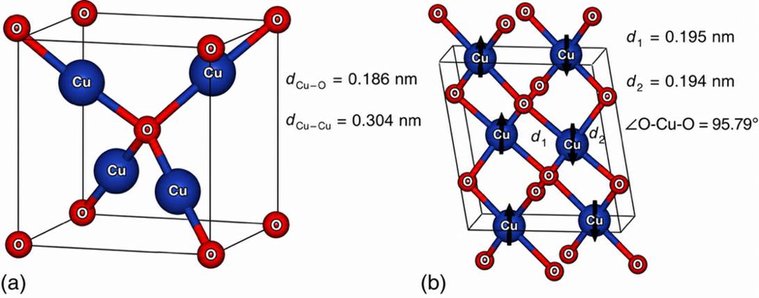
Figure 7 Crystal structure of binary copper oxides. (a) Cubic Cu2O and (b) Monoclinic CuO.
SnO
Recently, tin monoxide (SnO) has garnered significant attention due to its inherent p-type conductivity, structural stability, and electric properties in ambient environment. The bandgap of SnO ranges from 2.2 to 3.0 eV at 300 K. Figure 8 illustrates the crystal structure of SnO and the hybridization of valence-band maximum (VBM).
It is worth noting that the energy level of Sn 5s is in close proximity to that of O 2p near the VBM, as well as Sn 5p near the conduction band. This arrangement effectively reduces hole localization and results in high hole mobility.
The presence of Sn vacancies and oxygen interstitials contributes to the p-type conductivity observed in SnO. The native p-type behavior of SnO makes it suitable for various applications in the fields of TFTs, gas sensors, and optoelectronics.
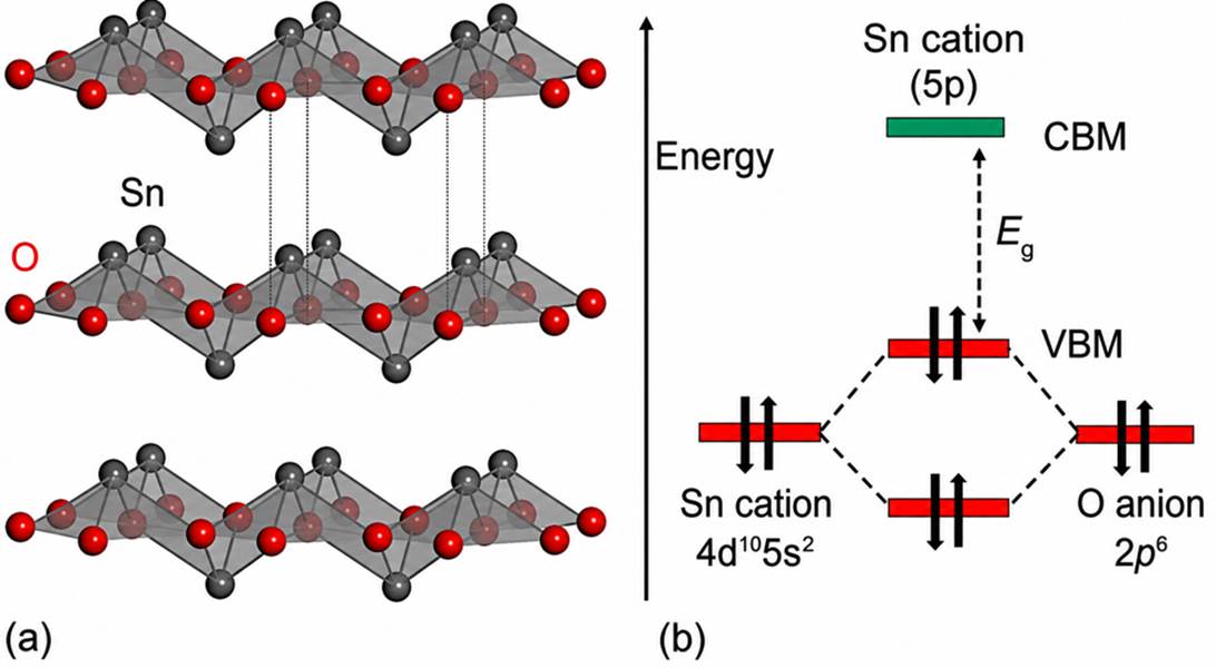
Figure 8 (a) Crystal structure of SnO. (b) Schematic illustration of the valence-band maximum (VBM) hybridization in SnO.
NiOx
NiOx is a widely studied p-type semiconductor that exhibits a green color in ambient environments and possesses a wide bandgap ranging from 3.6 to 4.0 eV. Due to its exceptional thermodynamic stability and unique optical/chemical properties, NiOx has attracted significant research interest in various fields, including solar cells, supercapacitors, catalysis, electrodes for lithium-ion batteries, and gas sensors.
Figure 9a illustrates the crystal structure of NiO. A sol–gel synthesis method can be used to prepare NiO thin films. In this typical procedure, nickel acetate serves as the source of Ni, and the flow diagram for the production of NiO films is depicted in Figure 9b. The NiO films prepared through this process and subsequently sintered at 700 °C exhibited an electron carrier concentration and mobility of 3.75 × 1019 cm−3 and 4.2 × 10⁻⁵ cm2 V−1s−1, respectively, along with a bandgap of 3.47 eV.
In various application scenarios like TFTs, photocatalysts, gas sensors, solar cells, and memristors, the morphological and structural characteristics of metal oxides play a crucial role in determining their performance. Factors such as crystal phases, terminal atom species, crystal size, shape, defects, vacancies, and crystal planes significantly influence the ultimate performance of these materials. Therefore, depending on the desired performance requirements, it is possible to design and improve the synthesis parameters while adhering to a fixed preparation strategy.
This approach allows us to obtain the desired metal oxide with specific properties, albeit with some compromises between performance merits such as sensitivity and stability.
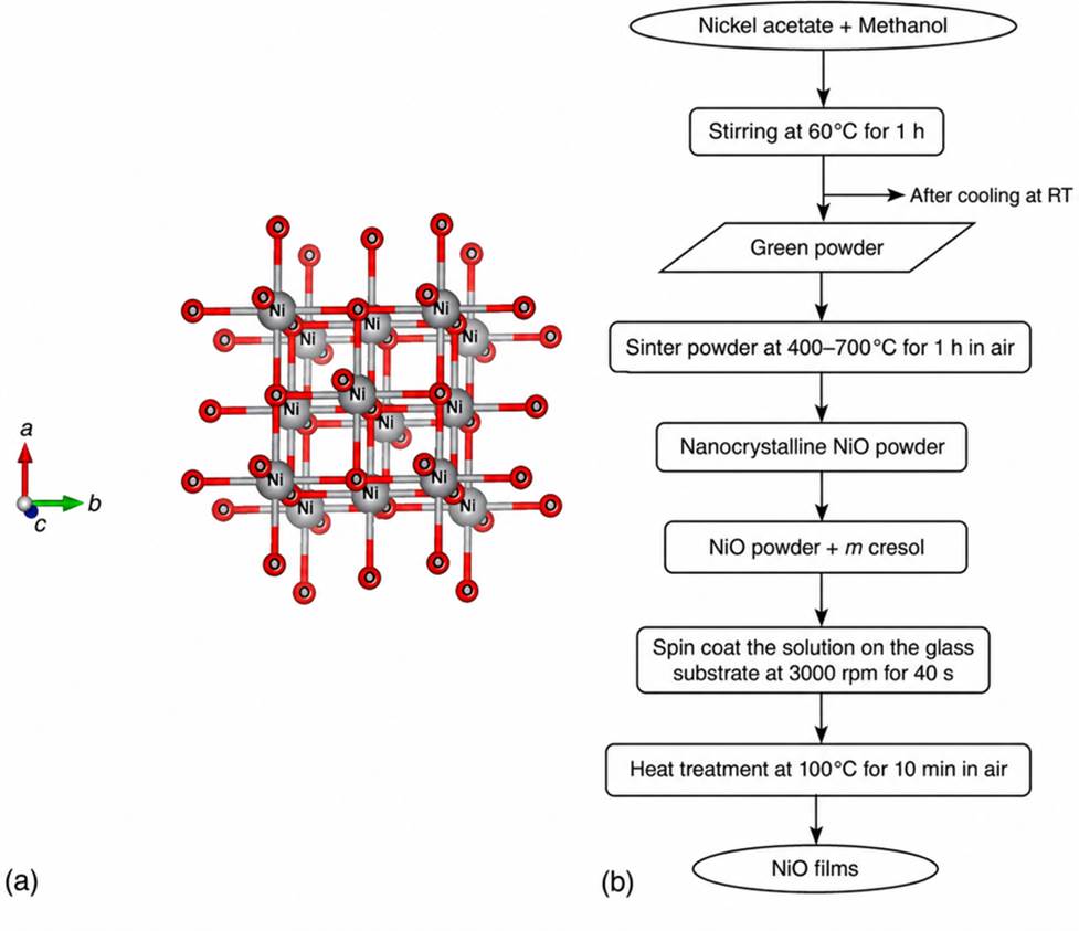
Figure 9 (a) Crystal structure of NiOx. (b) Flow diagram for NiO films synthesis by sol–gel method.
Key Takeaways
Metal oxide semiconductors (MOS) offer unique advantages over conventional semiconductors, including high optical transparency, mechanical flexibility, and strong electronic performance even in amorphous forms.
The article explores key n-type materials such as ZnO, SnO2, In2O3, TiO2, and Ga2O3, alongside p-type materials including CuO, Cu2O, SnO, and NiOx, highlighting their crystal structures, bandgaps, and functional properties. These semiconductors are widely used in applications such as thin-film transistors, gas sensors, solar cells, photocatalysts, memristors, and power electronics.
The article also emphasizes how morphology, crystal defects, phase structure, and synthesis methods directly influence the performance and reliability of metal oxide semiconductor devices.