Metallic Theta‑TaN Sets a New Benchmark for Heat Conduction
Researchers at Argonne National Laboratory have identified a metallic compound, θ-TaN, with thermal conductivity nearly three times that of copper, offering a new pathway for cooling AI, electronics, and quantum hardware.
Overheating smartphones and the rising thermal load from AI hardware expose the limits of today’s cooling pathways. These hotspots cap system performance, reliability, and efficiency.
Argonne National Laboratory’s Advanced Photon Source (APS) reports a metallic compound that changes the equation. A UCLA‑led team discovered theta‑phase tantalum nitride (θ‑TaN), a metal that conducts heat at roughly three times copper, pointing to new options for thermal design in high‑power electronics.
A metal that beats copper at its own job
The team measured a room-temperature thermal conductivity (k) — a measure of how efficiently a material conducts heat — near 1,100 W/m-K in θ-TaN. For reference, copper is near 400 W/m-K and has long served as the upper bound for metallic heat spreaders and heat sinks. The result sets a new record among metals and resets assumptions engineers hold about the practical ceiling for metallic thermal transport.
Why does this matter? Many emerging systems place localized heat sources under severe flux—think chiplet‑based AI accelerators, stacked memory, and compact power converters. A threefold conductivity jump in a metal suggests thinner spreaders, shorter lateral heat paths, and lower junction‑to‑case gradients without turning to brittle ceramics or costly diamond composites.
Electron–phonon coupling turned down
Metals carry heat through both electrons and phonons, but electron–phonon scattering usually throttles the net conductivity. In θ‑TaN, high‑resolution measurements show those interactions are unusually weak, allowing heat to flow far more freely than in conventional metals. That microscopic picture aligns with theory and helps explain the outsized bulk k observed.
The atomic arrangement appears to be central. Modeling indicates a distinctive hexagonal ordering of tantalum and nitrogen atoms that suppresses electron–phonon coupling and supports efficient carrier transport. The end result is a metallic nitride behaving more like an engineered heat superhighway than a typical refractory barrier.
How the team measured an outlier
Characterization relied on the upgraded APS, now among the world’s brightest synchrotron X‑ray sources. Researchers used the 30‑ID beamline—its first experiment post‑upgrade—to perform inelastic X‑ray scattering that directly probed phonon behavior and electron–phonon interactions. Ultrafast optical spectroscopy provided complementary time‑domain evidence for rapid heat flow. Together, these techniques tied the macroscopic conductivity to a clear microscopic mechanism.
The discovery was published in Science in January 2026 and highlighted by APS on April 13, 2026. That timeline reflects both the scientific peer review and the facility’s role in validating the transport physics with new instrumentation capabilities.
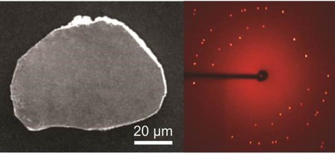
Electron microscopy image (left) and X-ray diffraction pattern (right) of a single crystal of theta-phase tantalum nitride.
What changes for thermal engineers
Heat spreaders and lids: A θ‑TaN spreader could reduce in‑plane temperature rise versus copper at the same thickness, or enable thinner lids without sacrificing performance. That can reclaim z-height—the vertical thickness—in dense packages and lower thermal resistance in stacked modules.
Hotspot control: Local inserts, heat shunts, or interposers fabricated from θ‑TaN may flatten gradients near chiplet edges or power stages where current crowding occurs. Shorter lateral conduction distances can allow smaller or fewer vapor chambers.
Materials tradeoffs: Being metallic, θ‑TaN avoids some interface penalties seen with ceramics. It can, however, introduce electrical conduction where insulation is required, so designs may need dielectric coatings or isolation layers to manage EMI and leakage.
System‑level impact: Data centers and AI clusters dominated by copper heat‑sinks and cold plates could see weight, footprint, or pump‑power reductions if spreader efficiency improves upstream of the coolant. Aerospace and quantum systems, both heat‑flux limited and integration sensitive, are similar beneficiaries.
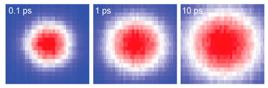
A sequence illustrating how electron-driven thermal energy spreads through theta-phase tantalum nitride after the material is stuck by a light pulse, spanning 0.1 to 10 picoseconds.
Integration questions engineers will ask next
Scalable manufacturing and form factors: The announcements do not yet detail routes to produce θ‑TaN as bulk plates, foils, or thin films at industrial scale. Deposition method, grain control, and phase stability will determine whether the lab performance carries into manufacturable parts.
Stability, reliability, and interfaces: Long‑term oxidation behavior, thermal cycling, and compatibility with solders, TIMs, and vapor‑chamber working fluids are open questions. Contact resistances could dominate if surfaces are difficult to passivate or polish—especially in thin‑film applications.
Mechanical and thermal‑mechanical properties: Coefficient of thermal expansion, yield strength, and hardness matter as much as k in real packages. Engineers will want a full property set to judge warpage, delamination risk, and machining or sputtering feasibility.
Electrical considerations: High k in a conductive metal is a double‑edged sword. Designs may prefer grounded spreaders or require dielectric barriers to control stray currents while preserving low thermal resistance.
Why this discovery lands now
The timing reflects both demand and tools. AI accelerators and high‑bandwidth memory generate concentrated heat loads that push copper close to its practical limits, while the APS upgrade delivered the resolution needed to connect macroscopic k with microscopic scattering physics. That combination enabled a credible path from “interesting crystal” to “engineering‑relevant material.” Notably, copper accounts for about 30% of commercial thermal‑management materials today—a market share that could shift if θ‑TaN proves scalable.
Outlook
Theta‑phase tantalum nitride expands the thermal‑management palette by demonstrating a metal with ~1.1 kW/m-K conductivity and a mechanistic rationale grounded in weak electron–phonon coupling. If industry can fabricate stable plates or films, qualify interfaces, and prove reliability, θ‑TaN could displace copper in the hottest zones of packages and systems. The first deployments are likely near AI, data centers, aerospace, and quantum platforms where every kelvin of margin matters. For now, the physics is sound, the measurements are modern, and the engineering opportunity is clear.