Nanotechnology Fabrication Methods: Top-Down Vs. Bottom-Up Approach
Learn how top-down and bottom-up nanotechnology fabrication methods enable the creation of nanoscale devices, advanced semiconductor structures, and next-generation materials for electronics, energy, and emerging technologies.
Nanotechnology fabrication relies on two primary methodologies: top-down (sculpting bulk materials into nano-scale structures) and bottom-up (assembling individual atoms or molecules into larger nanostructures). These methods enable the production of highly precise, efficient devices used in modern electronics, medicine, and energy systems.
Top-Down Approach
There are two general approaches involved in the implementation of nanotechnology. The first is the "top-down" approach and entails the use of fabrication processes and techniques to shape and form nano-dimensional scale elements from larger-sized sections of material.
The top-down approach involves production techniques that are largely equivalent to those used in the IC and microsystems industries and include deposition of thin films (perhaps having thicknesses in the nanometer range), lithography to make desired patterns in a photosensitive polymer layer, and etching.
An example of a process flow for the implementation of a nano-dimensional mechanical resonator device using these techniques is illustrated in Figure 1.
The fabrication process begins with a substrate that is usually made of single-crystal silicon (Figure 1a). Semiconductor substrates have developed to unparalleled levels of flatness and smoothness and these attributes are important when attempting to make nano-dimensional-sized features.
Subsequently, a thin-film material layer is deposited (Figure 1b). This layer is termed a "sacrificial layer" since it will not be employed in the device structure, but instead it will act as a standoff between the resonator and the substrate and will be removed at the end of the fabrication process. A typical sacrificial layer would be a thin-film layer of silicon dioxide (SiO2).
Next, another thin-film layer is deposited (Figure 1c). This layer is termed a "structural layer" because it will be the material from which the resonator is made. A typical structural layer would be polycrystalline silicon (also commonly referred to as "polysilicon").
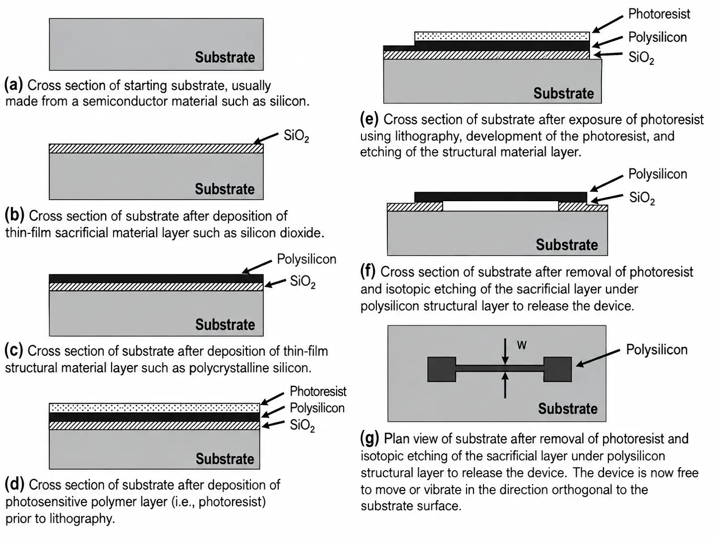
Figure 1 Process flow for the fabrication of a nano-mechanical resonator to illustrate a top-down approach to nanotechnology implementation.
There are a number of deposition processes that can be used to deposit the thin-film layers including CVD, physical vapor deposition that includes sputtering and evaporation, atomic layer deposition (ALD), spin coating, molecular beam epitaxy, and others. Note that some of these technologies are defined as "bottom-up" nanotechnologies.
The thin-film layer is then patterned using the methods of lithography (Figure 1d and e). There are a number of different technologies that can be used in lithography including optical photolithography, electron beam (e-beam) lithography, and imprint lithography. In the present example, we assume that we are using e-beam lithography.
Prior to performing e-beam lithography, a photo-sensitive polymer layer, called photoresist, is deposited onto the substrate surface using spin coating (Figure 1d). The thin-film structural material layer is etched using a dry plasma reactive ion etch process.
The photoresist is then removed by a plasma ashing process (Figure 1e).
Finally, the sacrificial material layer is removed using a gas-phase etchant such as vapor hydrofluoric acid. This releases the structural layer so that it can mechanically move and completes the fabrication process. The cross section and plan view of the nanoscale resonator is shown in Figure 1f and g, and the width of the resonator is labeled as "w."
It should be noted that the fabrication process illustrated in Figure 1 is only one of the methods to make a nanoscale device using a top-down approach.
Top-Down Approach Example – FinFET Transistor
Perhaps the most well-known, and certainly to date, the most commercially successful example of a top-down fabrication of a nanotechnology device is the FinFET transistor technology that is used in the manufacturing of state-of-the-art ICs.
A FinFET, also termed a fin field effect transistor (FET), is a nonplanar metal-oxide semiconductor (MOS) transistor technology that is extensively used for state-of-the-art microprocessors. The critical dimension of a transistor is the gate length, and the current generation of FinFET technology on the market has gate lengths of 14 nm.
The notable attribute of a FinFET is the fin of single crystal silicon semiconductor material that has a relatively high aspect ratio that protrudes from the substrate surface as shown in Figure 2.
Figure 2b is a three-dimensional illustration of the FinFET device topology. As can be seen, like a conventional MOS transistor there is a source, drain, and gate. However, unlike a conventional MOS device, the source and drain are connected by a thin, but high aspect ratio (height is larger than the width) fin of silicon. The fin acts as the channel for the flow of charge carriers (either electrons or holes) from the source to the drain. The flow of charge carriers in the fin is modulated by the gate voltage potential.
The gate overlaps the fin, but has a very thin dielectric to insulate the gate electrode from the fin as shown in Figure 2a. The gate material is an electrically conductive material layer. Importantly, the gate overlaps the fin on three sides, the top and the two sides. Consequently, sometimes this structure is called a tri-gate structure. This tri-gate configuration allows the gate voltage to have improved control capability overcharge carriers in the fin. The gate length is approximately the dimension given by "w" in Figure 2 and would be approximately 14 nm for the latest generation of the FinFET technology.
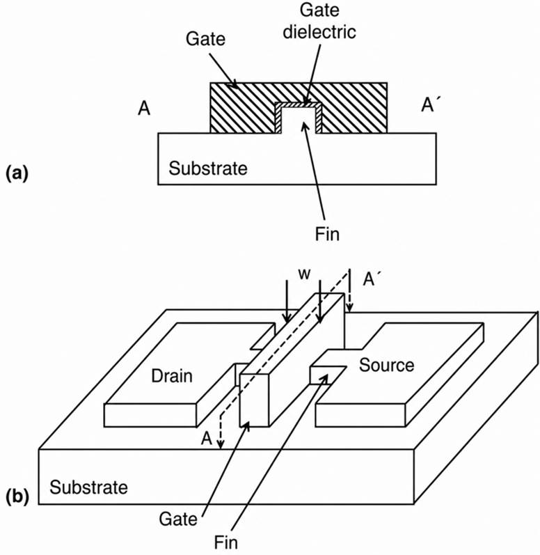
Figure 2 An illustration of the FinFET transistor. Shown in Figure 2b is a 3D representation of an individual FinFET transistor with a single fin. The source, drain, and fin are all made from single-crystal silicon. The fin is a high aspect ratio channel connecting the source and drain, where the charge carriers can flow. As shown in Figure 2a, the fin is coated in the thin dielectric layer and then with the gate material layer, which is usually an electrically conductive material. Because the voltage on the gate creates an electrical field from both sides and the top, this configuration is also called the tri-gate transistor.
Additionally, the FinFET structure allows multiple fins to be used in each transistor (to further improve the "on" currents), and higher packing densities. Intel claimed with the introduction of the Ivy Bridge 22 nanometer microprocessor that first used the FinFET technology, that a major redesign of the transistor structure was needed in order to continue Moore's law to the 22-nm node. The FinFET structure allowed them to extend Moore's law to 22 nm, then to the present 14-nm node, and it is expected to allow them to continue this path for several more years.
It is important to note that these are only two examples of top-down approaches to the implementation of nanotechnology. Specifically, there are other tools and approaches that can be used and more technologies are being developed each year. Another important point is that top-down approaches typically do not have atomic-level of control.
Bottom-Up Approach
The second approach to implementing nanotechnology is the bottom-up approach, which for all practical purposes means the engineered assembly of atoms or molecules to form nanoscale or larger objects. An example of the bottom-up approach would be the design of molecules having a specified shape and molecular recognition whereby individual molecules automatically self-assemble into a particular system configuration.
One example of the bottom-up approach to nanotechnology is ALD. ALD is a thin film deposition technique that uses sequential and self-limiting gas phase chemical processes. The reactant process gases are called precursors and each reacts with the existing surface onto which the material layer is being depositing in a self-limiting fashion. Typically, two precursor gases are used in ALD and neither is introduced into the deposition chamber at the same time. One precursor is introduced and reacts in a self-limited fashion with the substrate and once completed, the next phase is started wherein the second precursor is introduced to react with the substrate in a self-limited fashion, and so on.
The ALD process is illustrated in Figure 3.
- The substrate onto which the ALD layer is to be deposited is first placed into a reactor chamber (Figure 3a).
- The first precursor is introduced into the reactor chamber and reacts with the substrate surface to form a monolayer of a chemical species on the surface (Figure 3b).
- After the first precursor monolayer deposition is completed, any excess precursor gas is removed from the chamber (Figure 3c).
- Next, as shown in Figure 3d, the second precursor is introduced into the process chamber and starts to deposit a monolayer on the surface of the first precursor monolayer.
- Once the second precursor has completed the deposition of a monolayer, the excess process gas is removed (Figure 3e).
This process can be continued any number of times to create a thin film layer of desired thickness.
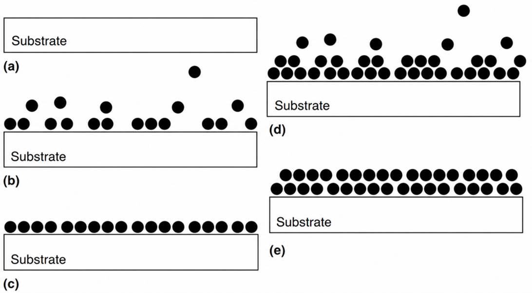
Figure 3 Illustration of the process in atomic layer deposition (ALD).
The advantages of ALD over conventional CVD are that ALD layers are extremely conformal, highly uniform, and have thicknesses that can be well controlled. A number of material types can be deposited using ALD, including SiO2, Al2O3, ZrO2, HfO2, TiN, TaN, Pt, Ti, and others.
A disadvantage of ALD is the low growth rate. ALD is now one of the principal deposition technologies now used in IC manufacturing to deposit the gate dielectric material layer in modern FinFET transistors. Typically, these layers are a high-k dielectric such as HfO2.
Bottom-Up Approach Example – Carbon Nanotubes
Perhaps the most notable examples of the bottom-up approach to nanotechnology are carbon nanotubes and other carbon-based molecules of the fullerene family.
Carbon nanotubes are one of many allotropes of carbon that can be single-walled nanotubes or multi-walled nanotubes, wherein there are concentric tubes of graphene (as in the so-called Russian Doll model) or a sheet of graphene rolled around itself (as in the so-called Parchment model).
Figure 4 illustrates a number of different allotropes of carbon, including diamond; graphite; fullerenes; C60 carbon fullerene molecule, which is also called a buckyball; and single-walled carbon nanotube.
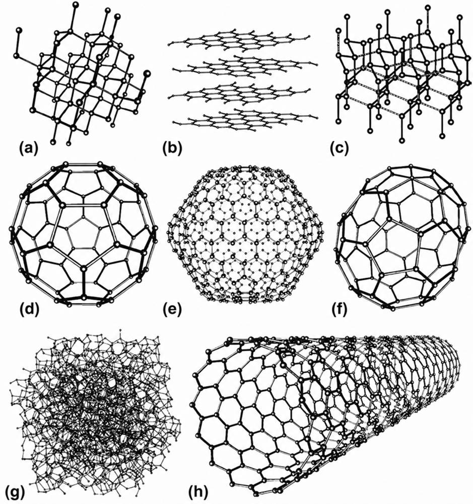
Figure 4 An illustration of several different types of allotropes of carbon molecules including (a) diamond, (b) graphite (single atomic layer of molecular carbon), (c) lonsdaleite, (d) C60 or Buckminsterfullerene, also known as "buckyball," (e) C540 fullerene, (f) C70 fullerene, (g) amorphous carbon, and (h) single-walled carbon nanotube.
Single-walled carbon nanotubes have a nominal diameter of about 1 nm and have been made with truly exceptional length-to-diameter ratios of up to 132,000,000:1. These materials also exhibit outstanding material properties. For example, carbon nanotubes have the highest tensile strength (e.g., between 13 and 53 GPa) and elastic modulus (e.g., between 1 and 5 TPa) of any material reported.
Moreover, carbon nanotubes have a low value of density, thereby resulting in a specific strength of 48,000 kN⋅m⋅kg−1, the highest of any known material. The electrical properties of carbon nanotubes depend on their structure and can be metallic or semiconducting with a theoretical maximum current density of over 109 Å/cm2, which is about 1000 times the current density of copper.
It is important to note that carbon nanotubes are only conductive along the axis of the nanotube.
The thermal properties of carbon nanotubes also depend on the structure and direction of heat transport. Single-walled carbon nanotubes have been shown to have a thermal conductivity along the axis of the nanotube of about 3500 W⋅m−1⋅K−1 and have a thermal conductivity in the radial direction that is much lower, about 1.5 W⋅m−1⋅K−1.
Carbon Nanotubes Production
There are several techniques that have been demonstrated for the production of carbon nanotubes including arc discharge, laser ablation, and CVD, with CVD demonstrating the most promise for large scale production.
Using CVD growth, typically a substrate surface will be prepared by depositing a layer of a suitable catalyst material or having defined regions or sites of a catalyst on desired locations across the substrate surface.
The catalysts most often used for carbon nanotubes are nickel, cobalt, iron, or a combination of these materials. Importantly, the growth of the carbon nanotubes will be limited to only those regions on the substrate surface where the catalysts are present.
Moreover, the size and type of nanotube grown is dependent on the diameter of the catalyst site on the surface of the substrate with smaller-diameter catalysts resulting in single-walled nanotubes. Therefore, the use of catalysts allows the size, types, and locations of nanotubes to be reasonably controlled by using fabrication techniques to deposit and pattern the catalyst sites to the desired diameters and locations on the substrate surface.
The CVD growth process entails heating the substrate to about 700°C and then introducing process gases into the deposition chamber, such as ammonia, nitrogen, or hydrogen, as well as a carbon-containing gas, such as acetylene, ethylene, or methane.
The carbon nanotubes grow from the sites of the metal catalyst on the substrate surface. If the growth process is conducted in the presence of an electrical field within the process chamber, the growth of the nanotubes will follow the direction of the electrical field and thereby make it possible to grow vertically oriented carbon nanotubes from the surface catalyst sites. For example, if the process used for deposition is a plasma-enhanced CVD, then vertically oriented nanotubes can be grown.
It should also be noted that under very special conditions, vertically oriented carbon nanotubes have been demonstrated without using an electric field. However, this is only possible with an extremely dense array of surface catalyst sites. Water-assisted CVD growth in addition to catalysts has demonstrated exceptionally high growth rates when compared to the use of catalysts along.
Some bottom-up approaches have been termed as "biomimetic" because these methods seek to emulate biological systems used by nature. One notable example of this type of nanotechnology is "DNA nanotechnology" or "nucleic acid nanotechnology," which involves the design and implementation of nucleic acid structures.
As mentioned earlier, some of the new carbon-based materials are expected to have a huge impact on the future development of ICs. Some of these new materials, such as graphene, are being explored to replace traditional semiconductor materials such as silicon.
Graphene is one of the allotropes of carbon and has form of a two-dimensional, atomic layer thick sheet wherein the carbon atoms are arranged in a honeycomb lattice. Graphene has many extraordinary properties and behaves either like a metal or a semiconductor depending on the lattice structure.
Graphene is about 100 times stronger than steel (assuming a layer of steel having the same thickness as graphene of about 3.4 Å, it conducts heat and electricity extremely well, and it is nearly transparent). There are two known orientations of graphene. The first is the zigzag orientation, which always demonstrates metallic behavior, and the second is the armchair orientation, which can demonstrate semiconducting or metallic behavior depending on the chirality.
Graphene exhibits remarkable electron mobility at room temperature, with reported values in excess of 15,000 cm2⋅V−1⋅s−1 with the potential theoretical limit of 200,000 cm2⋅V−1⋅s−1, which is about 10 × 106 times greater than copper. The electron and hole mobilities are expected to be nearly the same value.
Already graphene has been demonstrated by researchers to implement transistor devices. Recently, IBM researchers reported the operation of graphene FET with the highest frequencies reported to date. The IBM team reported that the operation frequency increases with diminishing device dimensions and that they had measured a graphene transistor cutoff frequency of 26 GHz with a gate length of 150 nm, the highest frequency obtained for graphene so far. Furthermore, by improving the gate dielectric materials, it is expected that the performance of these graphene transistors could be further improved, possibly obtaining terahertz graphene transistors with a gate length of 50 nm.
As this graphene example demonstrates, carbon-based nanotechnology materials are enabling higher performance ICs that are possible with conventional semiconductors. However, we are at the very early stages in the development of nanotechnology, and therefore it is not possible to accurately predict every possible implication of this new technology because new materials, fabrication methods, and devices are constantly being discovered that show great promise as well.
For example, researchers from the Swiss Federal Institute of Technology have created ICs using single-atom-thick molybdenite, a substance having properties similar to that of graphene. Molybdenite is a mineral composed of molybdenum disulfide, MoS2. Molybdenite in multiple layer form behaves as an indirect band gap semiconductor while a monolayer of this material has a direct band gap. Mobilities of 200 cm2⋅V−1⋅s−1 and room temperature current on/off ratios of 10 were reported. An image of the device is shown in Figure 5.
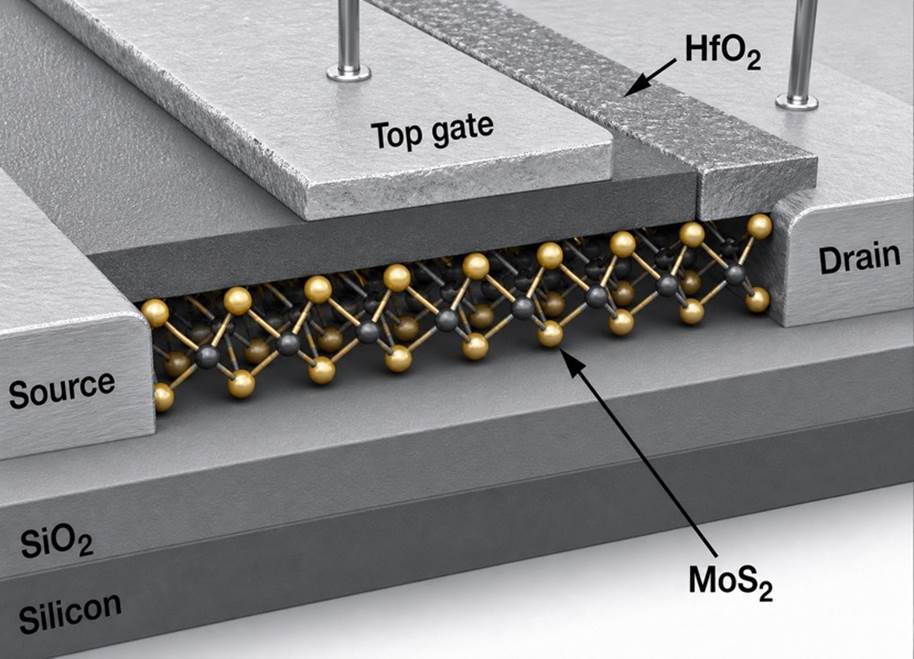
Figure 5 An illustration of an MoS2 transistor reported by the Swiss Federal Institute of Technology.
It is important to note that bottom-up approaches whereby larger structures or devices are made using these techniques are currently mostly limited to research endeavors and not actual products. Nevertheless, bottom-up approaches are used in the production of fullerenes and various nanoparticles (i.e., silver and gold) that are added to other materials to form compound mixtures that have enhanced material properties.
Key Takeaways
Nanotechnology manufacturing relies on two complementary approaches: top-down fabrication, which miniaturizes bulk materials through deposition, lithography, and etching processes, and bottom-up fabrication, which builds structures atom-by-atom or molecule-by-molecule with exceptional precision.
Top-down methods have driven the commercial success of advanced semiconductor technologies such as FinFET transistors, while bottom-up techniques including atomic layer deposition (ALD), carbon nanotube synthesis, graphene engineering, and DNA nanotechnology are opening new pathways for high-performance electronics and functional materials.
These fabrication strategies enable devices with greater speed, efficiency, strength, and miniaturization than conventional technologies. As research advances, nanoscale materials such as graphene, carbon nanotubes, and MoS₂ are expected to play a critical role in shaping the future of computing, sensing, energy systems, and next-generation integrated circuits.