Semiconductor Technologies for Transportation Electrification
Learn how silicon and wide-bandgap semiconductor technologies such as SiC and GaN are shaping high-efficiency, high-power electrified transportation systems.
In transportation electrification, Si‐MOSFETs are still being widely used in DC/DC converters, onboard charger (OBC) modules, as well as traction inverters. In terms of power, however, the Si‐MOSFETs are limited to converters with up to 10 s of kilowatts of power. For higher power applications, such as high voltage (HV) traction inverters that are used to drive >100 kW motors, the high conduction loss of Si‐MOSFETs is a limiting factor. Therefore, Si‐IGBTs were introduced.
Compared with Si‐MOSFETs that represent resistance when they are in on state, Si‐IGBTs are represented by a voltage source during on state. Therefore, although it is true that when IGBTs are on, the voltage drop across the IGBTs is at least one diode drop; however, compared with Si‐MOSFETs with the same rating, Si‐IGBTs exhibit a significantly lower on‐state conduction loss.
The reason for a lower conduction loss in Si‐IGBTs, as compared with Si‐MOSFETs, is the fact that unlike Si‐MOSFETs that are majority carrier devices where only electrons flow, in Si‐IGBTs, holes are injected into their drift region. Therefore, the electric current flow in an IGBT is composed of both electrons as well as holes.
The injection of holes as minority carriers significantly reduces the effective resistance of the IGBTs against current flow. In other words, conductivity is improved or equivalently the conduction loss is reduced.
As expected, nothing comes for free and the price paid for the higher conductivity of the IGBTs during on state and therefore lower conduction loss is their longer turn‐off time. The reason for a longer turn‐off time in Si‐IGBTs is that there is no effective way of stopping the holes as the device is turned off. The electron mobility is controlled by the voltage applied to the gate. Therefore, as the gate voltage is reduced to zero, the flow of electron is stopped. However, reducing the gate voltage does not remove the holes that are accumulated in the drift region. There is essentially no way to remove the holes from the drift region, unless by voltage gradient and recombination. This is the reason why Si‐IGBTs exhibit tail current during turn‐off events until all the holes are swept away or recombined.
The IGBT tailing current is shown in Figure 1. The big tail of current increases the turn‐off loss in IGBTs. The higher switching loss, in turn, results in a limitation on the application switching frequency to limit the excessive heat.
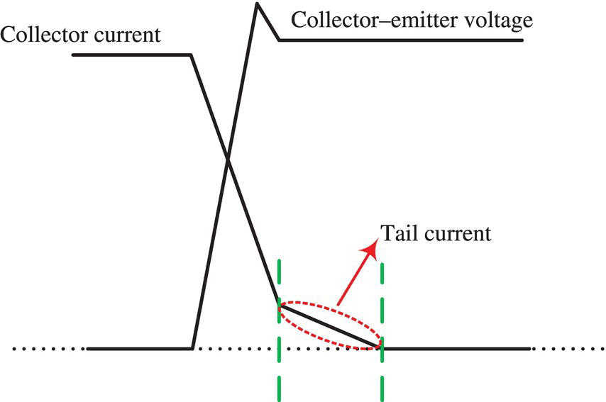
Figure 1 IGBT tail current during turn‐off results in high switching loss.
Trends in Transportation Electrification
As the electrification of transportation becomes mainstream in the automotive industry, efforts are made to improve efficiency and power density in high‐power electrified powertrains. Figure 2 shows a simplified schematic of a typical electrified powertrain.
In the schematic, shown in Figure 2, to increase efficiency, the HV battery voltage is increased. For the same power, a higher bus voltage means lower electric current, which then results in a lower copper loss and, therefore, higher efficiency.
On the other hand, to effectively increase the power density, the switching frequency must be increased. The increase in the switching frequency will result in a smaller DC‐link capacitor in traction inverters. The need for higher voltage and higher frequency capabilities in electrified powertrains resulted in the introduction of wide‐bandgap (WBG) devices such as SiC‐MOSFET and GaN devices.
Si Vs. SiC Vs. GaN Characteristics
Table 1 compares the main characteristics of silicon as a conventional semiconductor technology compared with SiC‐MOSFET and GaN as WBG devices.
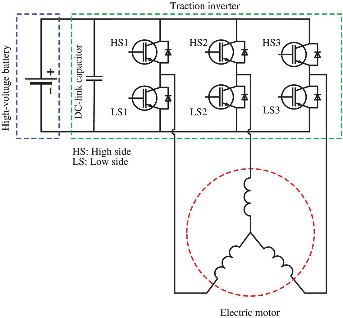
Figure 2 Simplified schematic of a typical electrified powertrain.
|
Properties |
Si |
SiC |
GaN |
|
Bandgap energy (eV) |
1.12 |
3.26 |
3.50 |
|
Electron mobility (cm2/Vs) |
1400 |
900 |
1250 |
|
Hole mobility (cm2/Vs) |
600 |
100 |
300 |
|
Breakdown field (MV/cm) |
0.3 |
3.0 |
3.0 |
|
Thermal conductivity (W/cm °C) |
1.5 |
4.9 |
1.3 |
|
Coefficient of thermal expansion (CTE) × 10−6 (°C−1) |
2.6 |
4.3 |
3.2 |
|
Maximum junction temperature (°C) |
150 |
600 |
400 |
Table 1 Comparing properties of Si vs SiC vs GaN
As seen in Table 1, the wider (three times higher) bandgap energy associated with SiC‐MOSFET and GaN devices means the energy to move electrons from their valence band to the conduction band is three times higher. Therefore, WBG devices behave more like an insulator and less like a conductor.
The higher bandgap energy in SiC‐MOSFETs and GaN devices allows them to withstand a much higher breakdown voltage (10 times higher) as compared with Si devices. The higher withstand voltage capability in WBG devices as compared with silicon enables a reduction in device thickness, which, by itself, translates into a lower on‐state resistance as well as higher power density at the die level.
The benefits associated with higher withstand voltage capability in WBG devices come at the expense of lower electron mobility. As seen in Table 1, the electron mobility in SiC is 64% of the electron mobility in Si. On the other hand, the hole mobility in SiC is only 17% of hole mobility in Si. Similar characteristics can be observed in the case of GaN devices. Therefore, although WBG devices have higher withstand voltage capabilities and therefore are better insulators, they are not great conductors. What this means from application's standpoint is that the gain of WBG devices is low as compared with silicon devices.
Comparing GaN vs SiC characteristics in Table 1, GaNs not only have slightly higher bandgap energy as compared with SiC but they also have higher electron mobility and higher hole mobility (both still lower than silicon). However, one of the key reasons why GaNs have not been able to penetrate high‐power applications such as electrified powertrains is the fact that they have a relatively low thermal conductivity. Based on Table 1, the thermal conductivity of GaN is ~15% lower compared with Si and ~75% lower compared with SiC.
A unique characteristic associated with GaN devices is that unlike Silicon and SiC‐MOSFET counterparts that are in enhancement mode, GaNs are in depletion mode in nature.
Enhancement mode devices are normally off devices that require a positive gate voltage to turn on. Depletion mode devices, on the other hand, are normally on and require a negative gate voltage to turn off.
Figure 3 shows the typical architecture of a depletion mode GaN. Because of the piezoelectric nature of GaN, two‐dimensional electron gas (2DEG) forms between GaN and AlGaN interface. The 2DEG layer provides a conductive path between the source and drain terminals and shorts them together. Therefore, the device is normally on at zero gate bias and requires a negative voltage to turn off.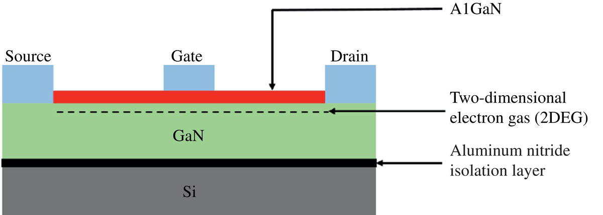
Figure 3 Typical depletion mode GaN/AlGaN architecture.
In power electronics applications, depletion mode devices are not preferred choices. Figure 4 shows a typical half‐bridge architecture, commonly used in power electronics applications including switched‐mode power supplies as well as traction inverters.
Since depletion mode GaN devices are normally on, that means they will cause a battery short circuit when no bias is present at their gate. Therefore, depletion mode GaNs cannot be used in such applications.
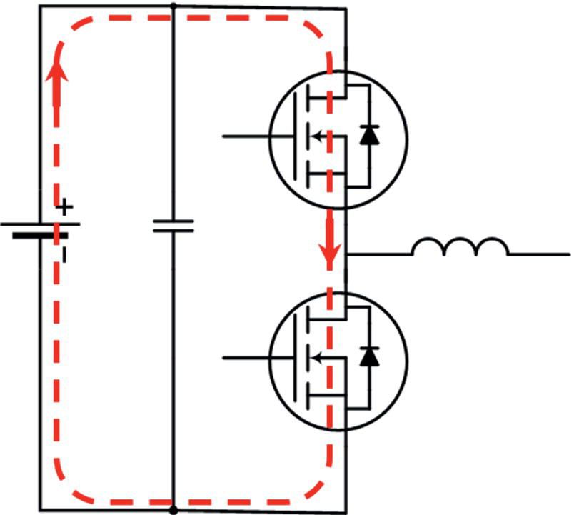
Figure 4 Typical half‐bridge architecture in power electronics applications.
Therefore, alternative approaches have been proposed by various GaN manufacturers to convert the depletion mode GaNs into enhancement mode GaNs. Figure 5 shows a GaN device in cascode configuration.
Cascode Configuration
In a cascode configuration, the high voltage (HV) GaN is placed in series with a low voltage (LV) silicon MOSFET. The GaN gate is grounded and the MOSFET gate is being driven to control the GaN device. Therefore, in addition to providing an enhancement mode functionality, this architecture also makes it possible to use typical silicon MOSFET gate drivers to drive the GaN device.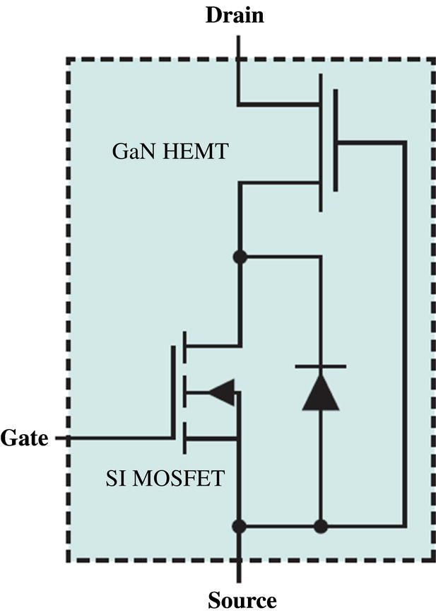
Figure 5 GaN device in cascode‐configuration.
The cascode architecture, despite its benefits, has practical challenges that make it an unfavorable solution.
- First of all, cascode GaN configuration exhibits higher parasitic capacitance since the GaN gate‐to‐source (CGS) capacitance and the Si‐MOSFET output capacitance (COSS) are placed in parallel. This jeopardizes one of the key advantages of the GaN devices, which is smaller parasitic capacitance and, therefore, faster switching capabilities.
- Second, in cascode configuration, the voltage distribution between the GaN and MOSFET in off mode can cause the MOSFET to avalanche. This is due to the lower drain‐to‐source capacitance (CDS) in the LV Si‐MOSFET as compared with the HV GaN device. One solution would be to add an external capacitor in parallel with the MOSFET's drain and source. However, this results in higher switching losses by slowing down the switching transitions.
Enhancement Mode GaN Architecture
Figure 6 shows an alternative enhancement mode GaN architecture, developed by efficient power conversion (EPC). In this architecture, there is a depletion region under the gate terminal that blocks the conductive path between the source and drain terminals. The eGaNs require a positive gate voltage above its threshold point to enhance the channel between the drain and source and conduct current.
Comparing the enhancement mode GaN (also known as eGaN) in Figure 6 vs depletion mode GaN (also known as dGaN) in Figure 3, one can notice that the fabrication process of eGaN is more complicated. However, the operation and control of eGaNs are much easier as compared with dGaNs. Therefore, eGaNs are preferred choices in power electronics applications.
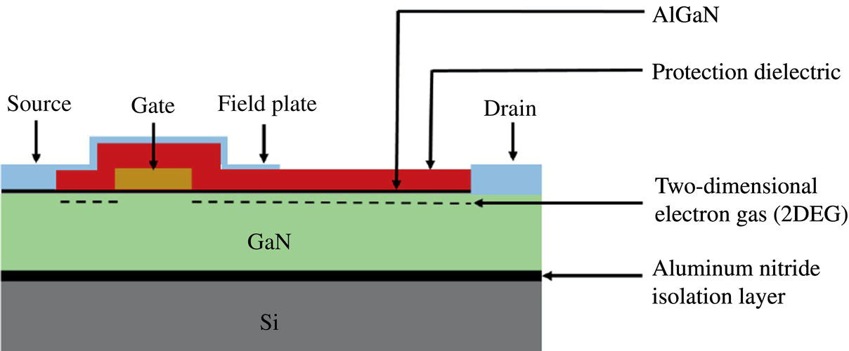
Figure 6 Enhancement mode GaN developed by EPC.
Key Takeaways
Silicon-based devices such as MOSFETs and IGBTs have long dominated power electronics, with IGBTs preferred in high-power applications due to lower conduction losses despite higher switching losses. The shift toward higher efficiency and power density in electrified transportation has driven adoption of wide-bandgap devices like SiC and GaN, which offer higher breakdown voltage, faster switching, and improved thermal performance. However, these advantages come with tradeoffs, including reduced carrier mobility and design challenges such as GaN’s native depletion-mode behavior and thermal limitations. As EV powertrains evolve toward higher voltages and switching frequencies, WBG devices are becoming essential for achieving compact, efficient, and high-performance systems.